- 您現(xiàn)在的位置:買賣IC網(wǎng) > PDF目錄378284 > ADC1251 (National Semiconductor Corporation) Self-Calibrating 12-Bit Plus Sign A/D Converter with Sample-and-Hold PDF資料下載
參數(shù)資料
| 型號: | ADC1251 |
| 廠商: | National Semiconductor Corporation |
| 英文描述: | Self-Calibrating 12-Bit Plus Sign A/D Converter with Sample-and-Hold |
| 中文描述: | 自校準12位帶符號的A / D轉(zhuǎn)換器的采樣保持電路 |
| 文件頁數(shù): | 12/16頁 |
| 文件大小: | 301K |
| 代理商: | ADC1251 |
2.0 Functional Description
(Continued)
A conversion sequence can also be controlled by the S/H
and CS inputs. Taking CS and S/H low starts the acquisition
window for the analog input voltage. The rising edge of S/H
immediately puts the A/D in the hold mode and starts the
conversion. Using S/H will simplify synchronizing the end of
the acquisition window to other signals, which may be nec-
essary in a DSP environment.
During a conversion, the sampled input voltage is succes-
sively compared to the output of the DAC. First, the ac-
quired input voltage is compared to analog ground to deter-
mine its polarity. The sign bit is set low for positive input
voltages and high for negative. Next the MSB of the DAC is
set high with the rest of the bits low. If the input voltage is
greater than the output of the DAC, then the MSB is left
high; otherwise it is set low. The next bit is set high, making
the output of the DAC three quarters or one quarter of full
scale. A comparison is done and if the input is greater than
the new DAC value this bit remains high; if the input is less
than the new DAC value the bit is set low. This process
continues until each bit has been tested. The result is then
stored in the output latch of the ADC1251. Next INT goes
low and EOC goes high to signal the end of the conversion.
The result can now be read by taking CS and RD low to
enable the DB0/DB8–DB7/DB12 output buffers. The high
byte of data is relayed first on the data bus outputs as
shown below:
DB0/
DB8
DB1/
DB9
DB2/
DB10
DB3/
DB11
DB4/
DB12
DB5/
DB12
DB6/
DB12
DB7/
DB12
Bit 8
Bit 9
Bit 10
MSB
Sign Bit
Sign Bit
Sign Bit
Sign Bit
Taking CS and RD low a second time will relay the low byte
of data on the data bus outputs as shown below:
DB0/
DB8
DB1/
DB9
DB2/
DB10
DB3/
DB11
DB4/
DB12
DB5/
DB12
DB6/
DB12
DB7/
DB12
LSB
Bit 1
Bit 2
Bit 3
Bit 4
Bit 5
Bit 6
Bit 7
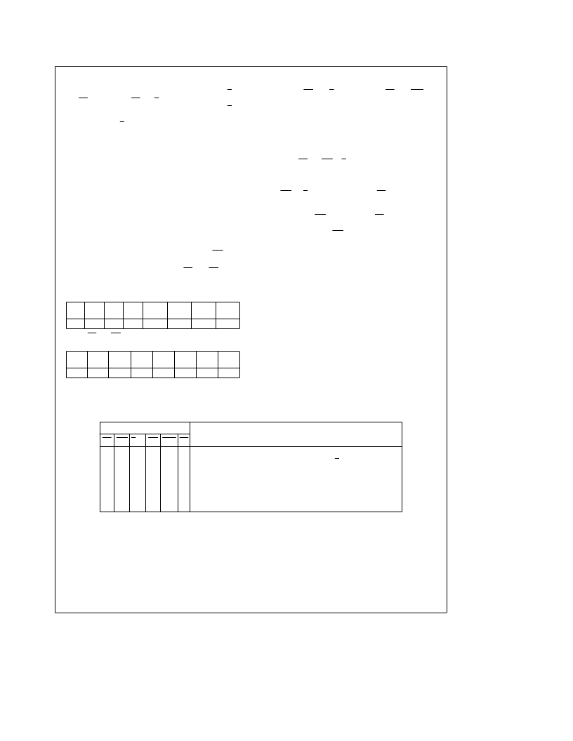
The table in Figure 3 summarizes the effect of the digital
control inputs on the function of the ADC1251. The Test
Mode, where RD and S/H are high and CS and CAL are
low, is used during manufacture to thoroughly check out the
operation of the ADC1251. Care should be taken not to in-
advertently be in this mode, since DB2, DB3, DB5, and DB6
become active outputs, which may cause data bus conten-
tion.
2.2 RESETTING THE A/D
The ADC1251 is reset whenever a new conversion is start-
ed by taking CS and WR or S/H low. If this is done when the
analog input is being sampled or when EOC is low, the
Auto-Cal correction factors may be corrupted, therefore re-
quiring an Auto-Cal cycle before the next conversion. When
using WR or S/H without Auto-Zero (AZ
e
1) to start a
conversion, a new conversion can be restarted only after
EOC has gone high, signaling the end of the current conver-
sion. When using WR with Auto-Zero (AZ
e
0) a new con-
version can be restarted during the first 26 clock periods
after the rising edge of WR (t
Z
) or after EOC has returned
high without corrupting the Auto-Cal correction factors.
The Calibration Cycle cannot be reset once started. On
power-up the ADC1251 automatically goes through a Cali-
bration Cycle that takes typically 1399 clock cycles. For rea-
sons that will be discussed in Section 3.8, a new calibration
cycle needs to be started after the completion of the auto-
matic one.
3.0 Analog Considerations
3.1 REFERENCE VOLTAGE
The voltage applied to the reference input of the converter
defines the voltage span of the analog input (the difference
between V
IN
and AGND), over which 4095 positive output
codes and 4096 negative output codes exist. The A-to-D
can be used in either ratiometric or absolute reference ap-
plications. The voltage source driving V
REF
must have a
very low output impedance and very low noise. The circuit in
Figure 4 is an example of a very stable reference that is
appropriate for use with the ADC1251.
Digital Control Inputs
A/D Function
CS WR S/H RD CAL AZ
1
0
1
1
1
1
1
1
1
1
1
1
1
0
0
X
X
Start Conversion without Auto-Zero
Start Conversion synchronous with rising edge of S/H without Auto-Zero
Read Conversion Result without Auto-Zero
Start Conversion with Auto-Zero
Read Conversion Result with Auto-Zero
Start Calibration Cycle
Test Mode (DB2, DB3, DB5, and DB6 become active)
1
1
1
1
1
1
X
1
X
1
1
X
X
0
FIGURE 3. Function of the A/D Control Inputs
12
相關(guān)PDF資料 |
PDF描述 |
|---|---|
| ADC1251CIJ | Self-Calibrating 12-Bit Plus Sign A/D Converter with Sample-and-Hold |
| ADC12662CIVF | 12-Bit, 1.5 MHz, 200 mW A/D Converter with Input Multiplexer and Sample/Hold |
| ADC12662 | 12-Bit, 1.5 MHz, 200 mW A/D Converter with Input Multiplexer and Sample/Hold |
| ADC12662CIV | 12-Bit, 1.5 MHz, 200 mW A/D Converter with Input Multiplexer and Sample/Hold |
| ADC12762 | 12-Bit, 1.4 MHz, 300 mW A/D Converter with Input Multiplexer and Sample/Hold |
相關(guān)代理商/技術(shù)參數(shù) |
參數(shù)描述 |
|---|---|
| ADC1251BIJ | 制造商:NSC 制造商全稱:National Semiconductor 功能描述:Self-Calibrating 12-Bit Plus Sign A/D Converter with Sample-and-Hold |
| ADC1251CIJ | 功能描述:IC ADC 12BIT W/S&H +SIGN 24CDIP RoHS:否 類別:集成電路 (IC) >> 數(shù)據(jù)采集 - 模數(shù)轉(zhuǎn)換器 系列:- 產(chǎn)品培訓(xùn)模塊:Lead (SnPb) Finish for COTS Obsolescence Mitigation Program 標準包裝:2,500 系列:- 位數(shù):12 采樣率(每秒):3M 數(shù)據(jù)接口:- 轉(zhuǎn)換器數(shù)目:- 功率耗散(最大):- 電壓電源:- 工作溫度:- 安裝類型:表面貼裝 封裝/外殼:SOT-23-6 供應(yīng)商設(shè)備封裝:SOT-23-6 包裝:帶卷 (TR) 輸入數(shù)目和類型:- |
| ADC1251CMJ | 制造商:NSC 制造商全稱:National Semiconductor 功能描述:Self-Calibrating 12-Bit Plus Sign A/D Converter with Sample-and-Hold |
| ADC1251CMJ/883 | 制造商:NSC 制造商全稱:National Semiconductor 功能描述:Self-Calibrating 12-Bit Plus Sign A/D Converter with Sample-and-Hold |
| ADC1255X | 制造商:未知廠家 制造商全稱:未知廠家 功能描述:ADC1255X 10-Bit 250KSPS SAR ADC|Data Sheet |
發(fā)布緊急采購,3分鐘左右您將得到回復(fù)。