- 您現(xiàn)在的位置:買(mǎi)賣(mài)IC網(wǎng) > PDF目錄374017 > ADN2850ACP25 (ANALOG DEVICES INC) Nonvolatile Memory, Dual 1024 Position Programmable Resistors PDF資料下載
參數(shù)資料
| 型號(hào): | ADN2850ACP25 |
| 廠商: | ANALOG DEVICES INC |
| 元件分類(lèi): | 數(shù)字電位計(jì) |
| 英文描述: | Nonvolatile Memory, Dual 1024 Position Programmable Resistors |
| 中文描述: | DUAL 25K DIGITAL POTENTIOMETER, 3-WIRE SERIAL CONTROL INTERFACE, 1024 POSITIONS, QCC16 |
| 封裝: | 5 X 5 MM, LFCSP-16 |
| 文件頁(yè)數(shù): | 5/18頁(yè) |
| 文件大小: | 270K |
| 代理商: | ADN2850ACP25 |
第1頁(yè)第2頁(yè)第3頁(yè)第4頁(yè)當(dāng)前第5頁(yè)第6頁(yè)第7頁(yè)第8頁(yè)第9頁(yè)第10頁(yè)第11頁(yè)第12頁(yè)第13頁(yè)第14頁(yè)第15頁(yè)第16頁(yè)第17頁(yè)第18頁(yè)
PRELIMINARY TECHNICAL DATA
Nonvolatile Memory Programmable Resistors
Absolute Maximum Rating
1
(
T
A
= +25°C, unless
otherwise noted)
V
DD
to GND............................................................-0.3V, +7V
V
SS
to GND ............................................................+0.3V, -7V
V
DD
to V
SS
.........................................................................+7V
V
B
, V
W
to GND..................................... V
SS
-0.3V, V
DD
+0.3V
B
X
– W
X
.......................................................................±20mA
Intermittent
2
..................................................±20mA
Continuous...................................................±1.3mA
Digital Inputs & Output Voltage to GND.....-0.3V, V
DD
+0.3V
Operating Temperature Range
3
........................-40°C to +85°C
Maximum Junction Temperature (T
J MAX
)...................+150°C
Storage Temperature......................................-65°C to +150°C
Lead Temperature, Soldering
4
Vapor Phase (60 sec).......................................+215 °C
Infrared (15 sec)...............................................+220 °C
Thermal Resistance Junction-to-Ambient
θ
JA,
LFCSP-16........................................................35°C/W
ADN2850
REV PrH, 13, AUG 2001
5
TSSOP-16 ..................................................... 150°C/W
Thermal Resistance Junction-to-Case
θ
JC,
LFCSP-16............................................................. TBD
TSSOP-16 ....................................................... 28°C/W
Package Power Dissipation = (TJMAX - TA) /
θ
JA
NOTES
1. Stresses above those listed under Absolute Maximum Ratings may
cause permanent damage to the device. This is a stress rating; functional
operation of the device at these or any other conditions above those
listed in the operational sections of this specification is not implied.
Exposure to absolute maximum rating conditions for extended periods
may affect device reliability.
2. Maximum terminal current is bounded by the maximum current
handling of the switches, maximum power dissipation of the package,
and maximum applied voltage across any two of the B, and W terminals
at a given resistance.
3. Includes programming of Nonvolatile memory
4. Applicable to TSSOP-16 only. For LFCSP-16, please consult factory
for detail
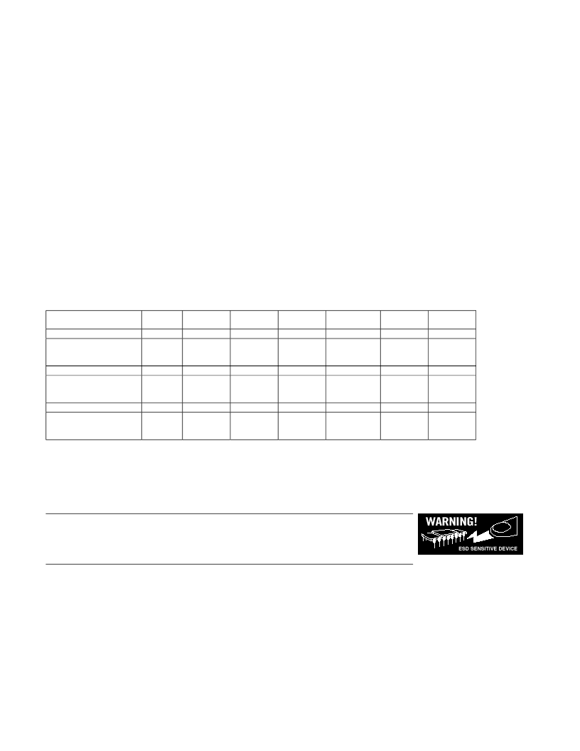
Ordering Guide
Model
R
WB
(k Ohm)
25
25
RDNL
(LSB)
±2
±2
RINL
(LSB)
±4
±4
Temp
Range
-40/+85°C
-40/+85°C
Package
Description
LFCSP-16
LFCSP-16
1500 Pieces
7” Reel
LFCSP-16
LFCSP-16
1500 Pieces
7” Reel
TSSOP-16
TSSOP-16
1000 Pieces
7” Reel
Package
Option
CP-16
CP-16
Top Mark*
ADN2850ACP25
ADN2850ACP25-RL7
ACP25
ACP25
ADN2850ACP250
ADN2850ACP250-RL7
250
250
±2
±2
±4
±4
-40/+85°C
-40/+85°C
CP-16
CP-16
ACP250
ACP250
ADN2850ARU25
ADN2850ARU25-REEL7
25
25
±2
±2
±4
±4
-40/+85°C
-40/+85°C
RU-16
RU-16
ARU25
ARU25
* Line 1 contains ADI logo symbol and date code YYWW, line 2 contains product number ADN2850, line 3 branding containing differentiating detail by part type, line
4 contains lot number.
CAUTION
ESD (electrostatic discharge) sensitive device. Electrostatic charges as high as 4000 V readily
accumulate on the human body and test equipment and can discharge without detection. Although the
ADN2850 features proprietary ESD protection circuitry, permanent damage may occur on devices
subjected to high-energy electrostatic discharges. Therefore, proper ESD precautions are recommended
to avoid performance degradation or loss of functionality.
相關(guān)PDF資料 |
PDF描述 |
|---|---|
| ADN2850ACP25-RL7 | Nonvolatile Memory, Dual 1024 Position Programmable Resistors |
| ADN2850ACP250 | TERM,RING NON-INSUL. |
| ADN2850ACP250-RL7 | Nonvolatile Memory, Dual 1024 Position Programmable Resistors |
| ADN2860 | High Bandwidth, CMOS 8-Bit Serial Interface Multiplying D/A Converter; Package: MSOP; No of Pins: 10; Temperature Range: Industrial |
| ADN2870 | High Bandwidth, CMOS 8-Bit Serial Interface Multiplying D/A Converter; Package: MSOP; No of Pins: 10; Temperature Range: Industrial |
相關(guān)代理商/技術(shù)參數(shù) |
參數(shù)描述 |
|---|---|
| ADN2850ACP250 | 制造商:AD 制造商全稱(chēng):Analog Devices 功能描述:Nonvolatile Memory, Dual 1024 Position Programmable Resistors |
| ADN2850ACP250-RL7 | 制造商:AD 制造商全稱(chēng):Analog Devices 功能描述:Nonvolatile Memory, Dual 1024 Position Programmable Resistors |
| ADN2850ACP25-RL7 | 制造商:AD 制造商全稱(chēng):Analog Devices 功能描述:Nonvolatile Memory, Dual 1024 Position Programmable Resistors |
| ADN2850ARU | 制造商:Analog Devices 功能描述:DUAL 10-BIT PROGRAMMABLE NON-VOLATILE RESISTOR - Bulk |
| ADN2850ARU25 | 制造商:AD 制造商全稱(chēng):Analog Devices 功能描述:Nonvolatile Memory, Dual 1024 Position Programmable Resistors |
發(fā)布緊急采購(gòu),3分鐘左右您將得到回復(fù)。