- 您現(xiàn)在的位置:買(mǎi)賣(mài)IC網(wǎng) > PDF目錄374017 > ADN8810-EVAL (Analog Devices, Inc.) 12-Bit High Output Current Source PDF資料下載
參數(shù)資料
| 型號(hào): | ADN8810-EVAL |
| 廠商: | Analog Devices, Inc. |
| 英文描述: | 12-Bit High Output Current Source |
| 中文描述: | 12位高輸出電流源 |
| 文件頁(yè)數(shù): | 13/16頁(yè) |
| 文件大?。?/td> | 232K |
| 代理商: | ADN8810-EVAL |
第1頁(yè)第2頁(yè)第3頁(yè)第4頁(yè)第5頁(yè)第6頁(yè)第7頁(yè)第8頁(yè)第9頁(yè)第10頁(yè)第11頁(yè)第12頁(yè)當(dāng)前第13頁(yè)第14頁(yè)第15頁(yè)第16頁(yè)
ADN8810
Rev. 0 | Page 13 of 16
DITHER
4.096V
R1
1.62k
R2
1.62k
C
1
μ
F
5V
AD8605
TO V
REF
0
Figure 19. Adding Dither to the Reference Voltage
Set the gain of the dither by adjusting the ratio of R2 to R1.
Increase C to lower the cutoff frequency of the high-pass filter
created by C and R1. The cutoff frequency of Figure 19 is
approximately 10 Hz.
The AD8605 is recommended as a low offset, rail-to-rail input
amplifier for this circuit.
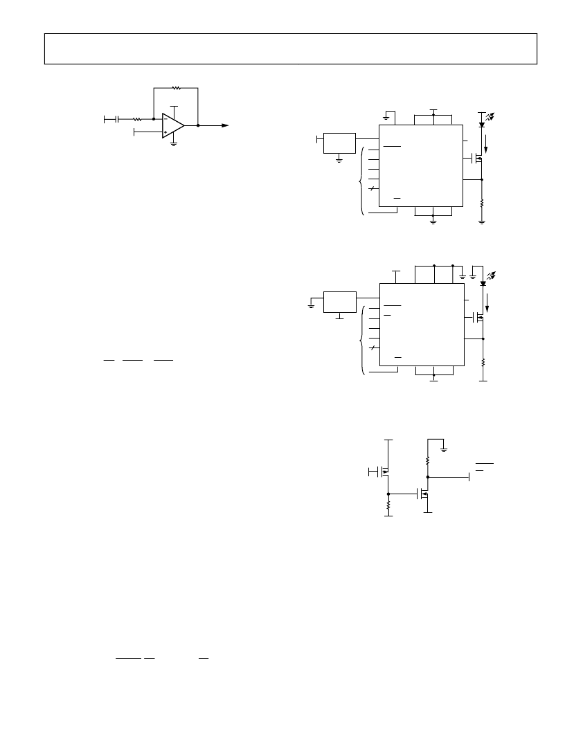
DRIVING COMMON-ANODE LASER DIODES
The ADN8810 can power common-anode laser diodes. These
are laser diodes whose anodes are fixed to the laser module
case. The module case is typically tied to either VDD or ground.
For common-anode-to-ground applications, a negative 5 V
supply must be provided.
In Figure 20, R
S
sets up the diode current by the equation
4096
5
16
1
1
1
×
096
.
Code
k
R
I
S
×
+
=
(5)
where
Code
is an integer value from 0 to 4,095. Using the values
in Figure 20, the diode current is 300.7 mA at a code value of
2,045 (0
x
7FF), or one-half full-scale. This effectively provides
11-bit current control from 0 mA to 300 mA of diode current.
The maximum output current of this configuration is limited by
the compliance voltage at the IOUT pin of the ADN8810. The
voltage at IOUT cannot exceed 1 V below PVDD, in this case
4 V. The IOUT voltage is equal to the voltage drop across R
S
plus
the gate-to-source voltage of the external FET. For this reason,
select a FET with a low threshold voltage.
In addition, the voltage across the R
S
resistor cannot exceed the
voltage at the cathode of the laser diode. Given a forward laser
diode voltage drop of 2 V in Figure 20, the voltage at the R
SN
pin
(I
×
R
S
) cannot exceed 3 V. This sets an upper limit to the value
of
Code
in Equation 5.
Although the configuration for anode-to-ground diodes is
similar, the supply voltages must be shifted down to 0 V and
–5 V, as shown in Figure. The AVDD, DVDD, and PVDD pins
are connected to ground with AVSS connected to –5 V. The
4.096 V reference must also be referred to the –5 V supply
voltage. The diode current is still determined by Equation 5.
All logic levels must be shifted down to 0 V and –5 V levels as
well. This includes RESET, CS, SCLK, SDI, SB, and all ADDR
pins. Figure shows a simple method to level shift a standard
TTL or CMOS (0 V to 5 V) signal down using external FETs.
FB
NC
D1
I = 300mA
@ CODE 0x7F
FDC633N
OR EQUIV
IOUT
R
SN
3
VOUT
VIN
GND
ADR292
R
6.81
NOTE: LEAVE FB WITH NO CONNECTION
ADN8810
5V
DGND
DVSS
AVSS
5V
5V
SB
PVDD
AVDD
DVDD
ENCOMP
ADDR0-2
SDI
SCLK
TTL/CMOS
LOGIC LEVELS
CS
RESET
VREF
0
Figure 20. Driving Common-Anode-to-VDD Laser Diodes
FB
NC
D1
I = 300mA
@ CODE 0x7F
FDC633N
OR EQUIV
IOUT
R
SN
3
VOUT
VIN
GND
ADR292
R
6.81
NOTE: LEAVE FB WITH NO CONNECTION
ADN8810
–5V
–5V
–5V
–5V
DGND
DVSS
AVSS
SB
PVDD
AVDD
DVDD
ENCOMP
ADDR0-2
SDI
SCLK
–5 TO 0V
LOGIC LEVELS
CS
RESET
VREF
0
Figure 21. Driving Common-Anode-to-Ground Laser Diodes with a Negative
Supply
NDC7003P
OR EQUIV
10k
100k
TO:
+3V
–5V
–5V
TTL/CMOS
LEVEL
RESET
CS
SCLK
SDI
NDC7002N
OR EQUIV
0
Figure 22. Level Shifting TTL/CMOS Logic
PC BOARD LAYOUT RECOMMENDATIONS
Although they can be driven from the same power supply
voltage, keep DVDD and AVDD current paths separate on the
PC board to maintain the highest accuracy; likewise for AVSS
and DGND. Tie common potentials together at a single point
located near the power regulator. This technique is known as
star grounding and is shown in Figure. This method reduces
digital crosstalk into the laser diode or load.
相關(guān)PDF資料 |
PDF描述 |
|---|---|
| ADN8810ACP | 12-Bit High Output Current Source |
| ADN8810ACP-REEL7 | 12-Bit High Output Current Source |
| ADN8820 | EDFA and CW Laser Controller |
| ADN8820-REEL7 | EDFA and CW Laser Controller |
| ADN8830 | Thermoelectric Cooler Controller |
相關(guān)代理商/技術(shù)參數(shù) |
參數(shù)描述 |
|---|---|
| ADN8810XCP | 制造商:Analog Devices 功能描述:- Bulk |
| ADN8820 | 制造商:Analog Devices 功能描述:LASER DRVR 1CH 48LFCSP - Trays |
| ADN8820ACP | 制造商:Analog Devices 功能描述:LASER DRVR 1CH 48LFCSP - Bulk |
| ADN8820-REEL7 | 制造商:AD 制造商全稱(chēng):Analog Devices 功能描述:EDFA and CW Laser Controller |
| ADN8830 | 制造商:AD 制造商全稱(chēng):Analog Devices 功能描述:Thermoelectric Cooler Controller |
發(fā)布緊急采購(gòu),3分鐘左右您將得到回復(fù)。