- 您現(xiàn)在的位置:買賣IC網(wǎng) > PDF目錄362147 > ADS8365IPAGRG4 16-Bit, 250kSPS, 6-Channel, Simultaneous Sampling SAR ANALOG-TO-DIGITAL CONVERTERS PDF資料下載
參數(shù)資料
| 型號: | ADS8365IPAGRG4 |
| 英文描述: | 16-Bit, 250kSPS, 6-Channel, Simultaneous Sampling SAR ANALOG-TO-DIGITAL CONVERTERS |
| 中文描述: | 16位,AD7691的6通道同步采樣SAR類比數(shù)位轉(zhuǎn)換器 |
| 文件頁數(shù): | 12/33頁 |
| 文件大小: | 441K |
| 代理商: | ADS8365IPAGRG4 |
第1頁第2頁第3頁第4頁第5頁第6頁第7頁第8頁第9頁第10頁第11頁當(dāng)前第12頁第13頁第14頁第15頁第16頁第17頁第18頁第19頁第20頁第21頁第22頁第23頁第24頁第25頁第26頁第27頁第28頁第29頁第30頁第31頁第32頁第33頁
www.ti.com
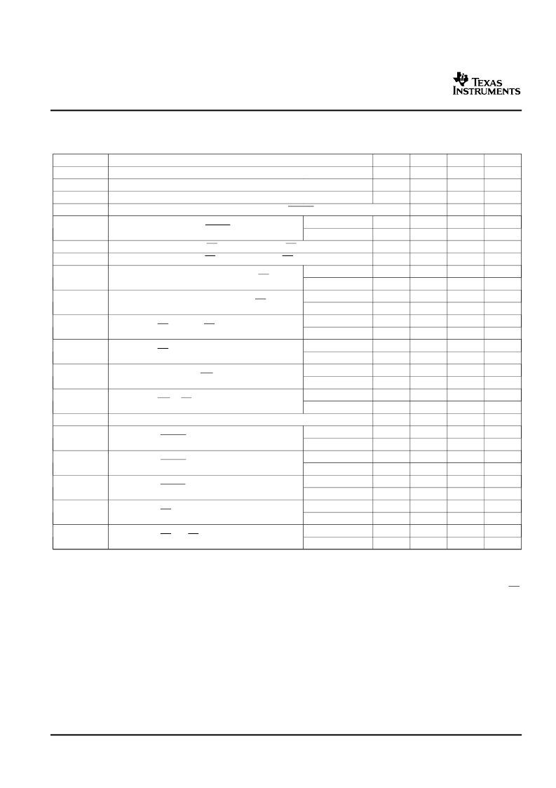
TIMING CHARACTERISTICS
(1)(2)(3)(4)
Over recommended operating free-air temperature range, T
MIN
to T
MAX
, AV
DD
= 5V, REF
IN
= REF
OUT
, V
REF
= internal +2.5V,
f
CLK
= 5MHz, f
SAMPLE
= 250kSPS, and BV
DD
= 2.7 to 5V, unless otherwise noted,
ADS8365
SBAS362A–AUGUST 2006–REVISED SEPTEMBER 2006
SYMBOL
t
ACQ
t
CONV
t
C1
t
D1(5)
DESCRIPTION
Acquisition time
Conversion time
Cycle time of CLK
Delay time of rising edge of CLK after falling edge of HOLDX
MIN
TYP
MAX
0.8
3.2
UNIT
μ
s
μ
s
ns
ns
ns
ns
ns
ns
ns
ns
ns
ns
ns
ns
ns
ns
ns
ns
ns
ns
ns
ns
ns
ns
ns
ns
ns
ns
ns
ns
ns
200
10
20
40
0
0
40
60
5
10
50
60
10
20
10
20
10
20
60
15
30
20
30
20
40
40
50
70
BV
DD
= 5V
BV
DD
= 3V
t
D2
Delay time of first hold after RESET
t
D4
t
D5
Delay time of falling edge of RD after falling edge of CS
Delay time of rising edge of CS after rising edge of RD
BV
DD
= 5V
BV
DD
= 3V
BV
DD
= 5V
BV
DD
= 3V
BV
DD
= 5V
BV
DD
= 3V
BV
DD
= 5V
BV
DD
= 3V
BV
DD
= 5V
BV
DD
= 3V
BV
DD
= 5V
BV
DD
= 3V
t
D6
Delay time of data valid after falling edge of RD
t
D7
Delay time of data hold from rising edge of RD
t
D8
Delay time of RD high after CS low
t
D9
Delay time of RD low after address setup
t
D10
Delay time of data valid to WR low
t
D11
Delay time of WR or CS high to data release
t
W1
Pulse width CLK high time or low time
BV
DD
= 5V
BV
DD
= 3V
BV
DD
= 5V
BV
DD
= 3V
BV
DD
= 5V
BV
DD
= 3V
BV
DD
= 5V
BV
DD
= 3V
BV
DD
= 5V
BV
DD
= 3V
t
W2
Pulse width of HOLDX high time to be recognized again
t
W3
Pulse width of HOLDX low time
t
W4
Pulse width of RESET
t
W5
Pulse width of RD high time
t
W6
Pulse width of RD and CS both low time
(1)
(2)
(3)
(4)
Assured by design.
All input signals are specified with rise time and fall time = 5ns (10% to 90% of BV
DD
) and timed from a voltage level of (V
IL
+ V
IH
)/2.
See
Figure 1
.
BYTE is asynchronous; when BYTE is 0, bits 15 to 0 appear at DB15 to DB0. When BYTE is 1, bits 15 to 8 appear on DB7 to DB0. RD
may remain LOW between changes in BYTE.
Only important when synchronization to clock is important.
(5)
12
Submit Documentation Feedback
相關(guān)PDF資料 |
PDF描述 |
|---|---|
| ADS8402IB | 16-BIT, 1.25 MSPS, UNIPOLAR DIFFERENTIAL INPUT, MICRO POWER SAMPLING ANALOG-TO-DIGITAL CONVERTER WITH PARALLEL INTERFACE AND REFERENCE |
| ADS8402 | 16-BIT, 1.25 MSPS, UNIPOLAR DIFFERENTIAL INPUT, MICRO POWER SAMPLING ANALOG-TO-DIGITAL CONVERTER WITH PARALLEL INTERFACE AND REFERENCE |
| ADS8402I | 16-BIT, 1.25 MSPS, UNIPOLAR DIFFERENTIAL INPUT, MICRO POWER SAMPLING ANALOG-TO-DIGITAL CONVERTER WITH PARALLEL INTERFACE AND REFERENCE |
| ADS8402IBPFBR | 16-BIT, 1.25 MSPS, UNIPOLAR DIFFERENTIAL INPUT, MICRO POWER SAMPLING ANALOG-TO-DIGITAL CONVERTER WITH PARALLEL INTERFACE AND REFERENCE |
| ADS8402IBPFBT | 16-BIT, 1.25 MSPS, UNIPOLAR DIFFERENTIAL INPUT, MICRO POWER SAMPLING ANALOG-TO-DIGITAL CONVERTER WITH PARALLEL INTERFACE AND REFERENCE |
相關(guān)代理商/技術(shù)參數(shù) |
參數(shù)描述 |
|---|---|
| ADS8365M-EVM | 功能描述:數(shù)據(jù)轉(zhuǎn)換 IC 開發(fā)工具 ADC CONVERTER RoHS:否 制造商:Texas Instruments 產(chǎn)品:Demonstration Kits 類型:ADC 工具用于評估:ADS130E08 接口類型:SPI 工作電源電壓:- 6 V to + 6 V |
| ADS8370 | 制造商:BB 制造商全稱:BB 功能描述:16-BIT, 600-kHz, PSEUDO-DIFFERENTIAL INPUT, MICROPOWER SAMPLING ANALOG-TO-DIGITAL CONVERTER WITH SERIAL INTERFACE AND REFERENCE |
| ADS8370EVM | 功能描述:數(shù)據(jù)轉(zhuǎn)換 IC 開發(fā)工具 ADS8370 Eval Mod RoHS:否 制造商:Texas Instruments 產(chǎn)品:Demonstration Kits 類型:ADC 工具用于評估:ADS130E08 接口類型:SPI 工作電源電壓:- 6 V to + 6 V |
| ADS8370I | 制造商:BB 制造商全稱:BB 功能描述:16-BIT, 600-kHz, PSEUDO-DIFFERENTIAL INPUT, MICROPOWER SAMPLING ANALOG-TO-DIGITAL CONVERTER WITH SERIAL INTERFACE AND REFERENCE |
| ADS8370IB | 制造商:BB 制造商全稱:BB 功能描述:16-BIT, 600-kHz, PSEUDO-DIFFERENTIAL INPUT, MICROPOWER SAMPLING ANALOG-TO-DIGITAL CONVERTER WITH SERIAL INTERFACE AND REFERENCE |
發(fā)布緊急采購,3分鐘左右您將得到回復(fù)。