- 您現(xiàn)在的位置:買賣IC網(wǎng) > PDF目錄374038 > ADT7518ARQZ-REEL (ANALOG DEVICES INC) SPI/I2C Compatible, Temperature Sensor, 4-Channel ADC and Quad Voltage Output DAC PDF資料下載
參數(shù)資料
| 型號: | ADT7518ARQZ-REEL |
| 廠商: | ANALOG DEVICES INC |
| 元件分類: | 溫度/濕度傳感器 |
| 英文描述: | SPI/I2C Compatible, Temperature Sensor, 4-Channel ADC and Quad Voltage Output DAC |
| 中文描述: | DIGITAL TEMP SENSOR-SERIAL, 10BIT(s), 5Cel, RECTANGULAR, SURFACE MOUNT |
| 封裝: | LEAD FREE, MO-137-AB, QSOP-16 |
| 文件頁數(shù): | 30/40頁 |
| 文件大?。?/td> | 1217K |
| 代理商: | ADT7518ARQZ-REEL |
第1頁第2頁第3頁第4頁第5頁第6頁第7頁第8頁第9頁第10頁第11頁第12頁第13頁第14頁第15頁第16頁第17頁第18頁第19頁第20頁第21頁第22頁第23頁第24頁第25頁第26頁第27頁第28頁第29頁當前第30頁第31頁第32頁第33頁第34頁第35頁第36頁第37頁第38頁第39頁第40頁
ADT7518
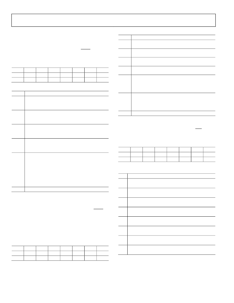
DAC Configuration Register (Read/Write)
[Address = 1Bh]
This configuration register is an 8-bit read/write register that is
used to control the output ranges of all four DACs and also to
control the loading of the DAC registers if the LDAC pin is
disabled (Bit C3 = 1, Control Configuration 3 register).
Rev. A | Page 30 of 40
Table 35. DAC Configuration
D7
D6
D7
D6
0*
0*
*
Default settings at power-up
Table 36.
Bit
Function
D0
Selects the output range of DAC A.
0 = 0 V to V
REF
.
1 = 0 V to 2V
REF
.
D1
Selects the output range of DAC B.
0 = 0 V to V
REF
.
1 = 0 V to 2V
REF
.
D2
Selects the output range of DAC C.
0 = 0 V to V
REF
.
1 = 0 V to 2V
REF
.
D3
Selects the output range of DAC D.
0 = 0 V to V
REF
.
1 = 0 V to 2V
REF
.
D5:D4 00 = A write to any DAC register generates LDAC
command that updates that DAC only.
01 = A write to DAC B or DAC D register generates
LDAC command that updates DACs A, B or DACs C, D,
respectively.
10 = A write to DAC D register generates LDAC
command that updates all four DACs.
11 = LDAC command generated from LDAC register.
D6:D7 Reserved. Write 0s only.
LDAC Configuration Register (Write-Only)
[Address = 1Ch]
This configuration register is an 8-bit write register that is used
to control the updating of the quad DAC outputs if the LDAC
pin is disabled and Bits D4:D5 of the DAC configuration reg-
ister are both set to 1. Also selects either the internal or external
V
REF
for all four DACs. Bits D0:D3 in this register are self-clear-
ing, i.e., reading back from this register will always give 0s for
these bits.
D5
D5
0*
D4
D4
0*
D3
D3
0*
D2
D2
0*
D1
D1
0*
D0
D0
0*
Table 37. LDAC Configuration
D7
D6
D7
D6
0*
0*
D5
D5
0*
D4
D4
0*
D3
D3
0*
D2
D2
0*
D1
D1
0*
D0
D0
0*
*
Default settings at power-up
Table 38.
Bit
D0
Function
Writing a 1 to this bit will generate the LDAC command
to update DAC A output only.
Writing a 1 to this bit will generate the LDAC command
to update DAC B output only.
Writing a 1 to this bit will generate the LDAC command
to update DAC C output only.
Writing a 1 to this bit will generate the LDAC command
to update DAC D output only.
Selects either internal V
REF
or external V
REF
for DACs A
and B.
0 = External V
REF
1 = Internal V
REF
.
Selects either internal V
REF
or external V
REF
for DACs C
and D.
0 = External V
REF
1 = Internal V
REF
Reserved. Write 0s only.
D1
D2
D3
D4
D5
D6:D7
Interrupt Mask 1 Register (Read/Write) [Address = 1Dh]
This mask register is an 8-bit read/write register that can be
used to mask any interrupts that can cause the INT/INT pin to
go active.
Table 39. Interrupt Mask 1
D7
D6
D7
D6
0*
0*
D5
D5
0*
D4
D4
0*
D3
D3
0*
D2
D2
0*
D1
D1
0*
D0
D0
0*
*
Default settings at power-up
Table 40.
Bit
Function
D0
0 = Enable internal T
HIGH
interrupt.
1 = Disable internal T
HIGH
interrupt.
D1
0 = Enable internal T
LOW
interrupt.
1 = Disable internal T
LOW
interrupt.
D2
0 = Enable external T
HIGH
interrupt or AIN1 interrupt.
1 = Disable external T
HIGH
interrupt or AIN1 interrupt.
D3
0 = Enable external T
LOW
interrupt.
1 = Disable external T
LOW
interrupt.
D4
0 = Enable external temperature fault interrupt..
1 = Disable external temperature fault interrupt.
D5
0 = Enable AIN2 interrupt.
1 = Disable AIN2 interrupt.
D6
0 = Enable AIN3 interrupt.
1 = Disable AIN3 interrupt.
D7
0 = Enable AIN4 interrupt.
1 = Disable AIN4 interrupt.
相關PDF資料 |
PDF描述 |
|---|---|
| ADT7518ARQZ-REEL7 | SPI/I2C Compatible, Temperature Sensor, 4-Channel ADC and Quad Voltage Output DAC |
| ADUC7020BCP62 | Precision Analog Microcontroller 12-bit Analog I/O, ARM7TDMI MCU |
| ADUC7021ACP32 | Precision Analog Microcontroller 12-bit Analog I/O, ARM7TDMI MCU |
| ADUC7021BCP32 | Precision Analog Microcontroller 12-bit Analog I/O, ARM7TDMI MCU |
| ADUC7021BCP62 | Precision Analog Microcontroller 12-bit Analog I/O, ARM7TDMI MCU |
相關代理商/技術參數(shù) |
參數(shù)描述 |
|---|---|
| ADT7518ARQZ-REEL7 | 制造商:Analog Devices 功能描述:Temp Sensor Analog Serial (4-Wire, SPI, I2C) 16-Pin QSOP T/R |
| ADT7519 | 制造商:AD 制造商全稱:Analog Devices 功能描述:SPI-/I2C-Compatible, Temperature Sensor,4-Channel ADC and Quad Voltage Output |
| ADT7519ARQ | 制造商:Analog Devices 功能描述:Temp Sensor Digital Serial (4-Wire, SPI, I2C) 16-Pin QSOP |
| ADT7519ARQ-REEL | 制造商:Analog Devices 功能描述:Temp Sensor Digital Serial (4-Wire, SPI, I2C) 16-Pin QSOP T/R |
| ADT7519ARQ-REEL7 | 制造商:Analog Devices 功能描述:Temp Sensor Digital Serial (4-Wire, SPI, I2C) 16-Pin QSOP T/R 制造商:Analog Devices 功能描述:TEMP SENSOR DGTL SERL (4-WIRE, SPI) 16QSOP - Tape and Reel |
發(fā)布緊急采購,3分鐘左右您將得到回復。