- 您現(xiàn)在的位置:買賣IC網(wǎng) > PDF目錄374038 > ADT7518ARQZ (ANALOG DEVICES INC) SPI/I2C Compatible, Temperature Sensor, 4-Channel ADC and Quad Voltage Output DAC PDF資料下載
參數(shù)資料
| 型號: | ADT7518ARQZ |
| 廠商: | ANALOG DEVICES INC |
| 元件分類: | 溫度/濕度傳感器 |
| 英文描述: | SPI/I2C Compatible, Temperature Sensor, 4-Channel ADC and Quad Voltage Output DAC |
| 中文描述: | DIGITAL TEMP SENSOR-SERIAL, 10BIT(s), 5Cel, RECTANGULAR, SURFACE MOUNT |
| 封裝: | LEAD FREE, MO-137-AB, QSOP-16 |
| 文件頁數(shù): | 34/40頁 |
| 文件大小: | 1217K |
| 代理商: | ADT7518ARQZ |
第1頁第2頁第3頁第4頁第5頁第6頁第7頁第8頁第9頁第10頁第11頁第12頁第13頁第14頁第15頁第16頁第17頁第18頁第19頁第20頁第21頁第22頁第23頁第24頁第25頁第26頁第27頁第28頁第29頁第30頁第31頁第32頁第33頁當前第34頁第35頁第36頁第37頁第38頁第39頁第40頁
ADT7518
Rev. A | Page 34 of 40
A
B
CS
(START HIGH)
SPI LOCKED ON
THIRD RISING EDGE
C
SPI FRAMING
EDGE
0
A
B
CS
(START LOW)
SPI LOCKED ON
THIRD RISING EDGE
C
SPI FRAMING
EDGE
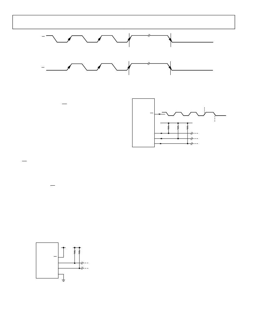
Figure 53. Serial Interface—Selecting and Locking SPI Protocol
To select and lock the interface into the SPI mode, a number of
pulses must be sent down the CS line (Pin 4). The following
section describes how this is done.
Once the SPI communication protocol has been locked in, it
cannot be unlocked while the device is still powered up. Bit D0
of the SPI lock status register (Address 7Fh) is set to 1 when a
successful SPI interface lock has been accomplished. To reset
the serial interface, the user must power down the part and
power it up again. A software reset does not reset the serial
interface.
Serial Interface Selection
The CS line controls the selection between I
2
C and SPI.
Figure 53 shows the selection process necessary to lock the SPI
interface mode.
To communicate to the ADT7518 using the SPI protocol, send
three pulses down the CS line as shown in Figure 53. On the
third rising edge (marked as C in Figure 53), the part selects and
locks the SPI interface. The user is now limited to communi-
cating to the device using the SPI protocol.
As per most SPI standards, the CS line must be low during
every SPI communication to the ADT7518 and high all other
times. Typical examples of how to connect the dual interface as
I
2
C or SPI is shown in Figure 54 and Figure 55. The following
sections describe in detail how to use the I
2
C and SPI protocols
associated with the ADT7518.
ADT7518
CS
SDA
SCL
ADD
V
DD
V
DD
I
2
C ADDRESS = 1001 000
10k
10k
0
Figure 54. Typical I
2
C Interface Connection
ADT7518
SCLK
DOUT
CS
V
DD
LOCK AND
SELECT SPI
SPI FRAMING
EDGE
820
820
820
DIN
0
Figure 55. Typical SPI Interface Connection
I
2
C Serial Interface
Like all I
2
C-compatible devices, the ADT7518 has a 7-bit serial
address. The four MSBs of this address for the ADT7518 are set
to 1001. The three LSBs are set by Pin 11, ADD. The ADD pin
can be configured three ways to give three different address
options: low, floating, and high. Setting the ADD pin low gives a
serial bus address of 1001 000, leaving it floating gives the
address 1001 010, and setting it high gives the address 1001 011.
The recommended pull-up resistor value is 10 k.
There is an enable/disable bit for the SMBus timeout. When this
is enabled, the SMBus will time out after 25 ms of no activity. To
enable it, set Bit 6 of the Control Configuration 2 register. The
power-on default is with the SMBus timeout disabled.
The ADT7518 supports SMBus packet error checking (PEC),
but its use is optional. It is triggered by supplying the extra
clocks for the PEC byte. The PEC is calculated using CRC-8.
The frame clock sequence (FCS) conforms to CRC-8 by the
polynominal
( )
1
1
2
8
+
+
+
=
x
x
x
C
Consult the SMBus specification (
www.smbus.org
) for more
information.
相關PDF資料 |
PDF描述 |
|---|---|
| ADT7518ARQZ-REEL | SPI/I2C Compatible, Temperature Sensor, 4-Channel ADC and Quad Voltage Output DAC |
| ADT7518ARQZ-REEL7 | SPI/I2C Compatible, Temperature Sensor, 4-Channel ADC and Quad Voltage Output DAC |
| ADUC7020BCP62 | Precision Analog Microcontroller 12-bit Analog I/O, ARM7TDMI MCU |
| ADUC7021ACP32 | Precision Analog Microcontroller 12-bit Analog I/O, ARM7TDMI MCU |
| ADUC7021BCP32 | Precision Analog Microcontroller 12-bit Analog I/O, ARM7TDMI MCU |
相關代理商/技術(shù)參數(shù) |
參數(shù)描述 |
|---|---|
| ADT7518ARQZ-REEL | 制造商:Analog Devices 功能描述:Temp Sensor Analog Serial (4-Wire, SPI, I2C) 16-Pin QSOP T/R |
| ADT7518ARQZ-REEL7 | 制造商:Analog Devices 功能描述:Temp Sensor Analog Serial (4-Wire, SPI, I2C) 16-Pin QSOP T/R |
| ADT7519 | 制造商:AD 制造商全稱:Analog Devices 功能描述:SPI-/I2C-Compatible, Temperature Sensor,4-Channel ADC and Quad Voltage Output |
| ADT7519ARQ | 制造商:Analog Devices 功能描述:Temp Sensor Digital Serial (4-Wire, SPI, I2C) 16-Pin QSOP |
| ADT7519ARQ-REEL | 制造商:Analog Devices 功能描述:Temp Sensor Digital Serial (4-Wire, SPI, I2C) 16-Pin QSOP T/R |
發(fā)布緊急采購,3分鐘左右您將得到回復。