- 您現(xiàn)在的位置:買賣IC網(wǎng) > PDF目錄362157 > AG203-86G InGaP HBT Gain Block PDF資料下載
參數(shù)資料
| 型號: | AG203-86G |
| 英文描述: | InGaP HBT Gain Block |
| 中文描述: | InGaP HBT增益模塊 |
| 文件頁數(shù): | 4/6頁 |
| 文件大?。?/td> | 446K |
| 代理商: | AG203-86G |
Specifications and information are subject to change without notice
WJ Communications, Inc
Phone 1-800-WJ1-4401 FAX: 408-577-6621 e-mail: sales@wj.com Web site: www.wj.com
Page 4 of 6 June 2005
AG203-86
InGaP HBT Gain Block
Product Information
The Communications Edge
TM
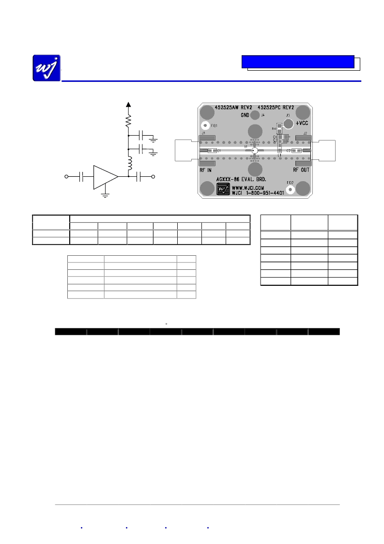
Application Circuit
Recommended Component Values
Reference
Designator
L1
C1, C2, C4
1. The proper values for the components are dependent upon the intended frequency of operation.
2. The following values are contained on the evaluation board to achieve optimal broadband performance:
Ref. Desig.
Value / Type
L1
39 nH wirewound inductor
C1, C2
56 pF chip capacitor
C3
0.018
P
F chip capacitor
C4
Do Not Place
R1
47.5
:
1% tolerance
Frequency (MHz)
900
1900
68 nH
27 nH
100 pF
50
500
220 nH
1000 pF
2200
22 nH
68 pF
2500
18 nH
56 pF
3500
15 nH
39 pF
820 nH
.018 μF
68 pF
Size
0603
0603
0603
0603
Recommended Bias Resistor Values
Supply
Voltage
5 V
47.5 ohms
6 V
98 ohms
7 V
148 ohms
8 V
198 ohms
9 V
248 ohms
10 V
298 ohms
12 V
398 ohms
The proper value for R1 is dependent upon the supply
voltage and allows for bias stability over temperature.
WJ recommends a minimum supply bias of +5 V. A
1% tolerance resistor is recommended.
R1 value
Size
0603
0603
0805
0805
1206
1210
1210
Typical Device Data
S-Parameters (V
device
= +4.05 V, I
CC
= 20 mA, T = 25 C, calibrated to device leads.
Freq (MHz)
S11 (dB)
S11 (ang)
50
-22.84
-0.07
250
-23.86
9.00
500
-27.29
28.82
750
-26.07
34.92
1000
-25.11
29.08
1250
-22.93
24.43
1500
-22.25
14.88
1750
-20.95
2.45
2000
-19.51
-8.95
2250
-16.43
-13.31
2500
-16.78
-23.33
2750
-16.30
-34.19
3000
-16.36
-40.45
3250
-17.08
-46.15
3500
-18.26
-50.28
3750
-20.54
-49.45
4000
-24.06
-47.33
4250
-26.27
-34.92
4500
-28.81
-7.87
4750
-29.10
4.10
5000
-29.66
-6.98
5250
-27.47
-47.93
5500
-23.43
-76.94
5750
-20.02
-92.84
6000
-17.60
-100.20
S21 (dB)
20.75
20.67
20.50
20.14
19.67
19.20
18.61
18.05
17.41
16.82
16.42
15.94
15.44
15.04
14.61
14.22
13.82
13.42
12.97
12.58
12.26
11.89
11.53
11.26
10.98
S21 (ang)
177.32
166.89
153.87
141.62
129.97
118.62
108.25
98.43
89.13
81.09
75.17
66.69
59.03
51.80
44.52
37.06
29.86
22.90
15.72
8.48
1.83
-4.38
-10.48
-16.74
-22.74
S12 (dB)
-23.39
-23.73
-23.63
-23.52
-23.71
-22.95
-23.00
-22.57
-22.18
-21.84
-22.12
-21.11
-20.69
-20.33
-19.98
-19.86
-19.34
-18.89
-18.65
-18.33
-17.90
-17.79
-17.36
-17.43
-17.06
S12 (ang)
0.76
2.56
1.56
1.40
-0.82
0.96
-0.16
1.41
2.42
-1.23
-6.06
-6.07
-4.81
-6.56
-9.18
-14.94
-14.68
-20.14
-21.13
-26.55
-29.89
-34.21
-36.99
-39.01
-44.67
S22 (dB)
-13.40
-13.66
-15.89
-16.64
-17.55
-17.47
-17.07
-16.20
-15.55
-13.16
-13.53
-14.17
-15.24
-16.92
-19.42
-22.27
-21.48
-19.26
-17.44
-15.98
-14.84
-15.32
-15.49
-15.72
-15.62
S22 (ang)
-3.20
-11.48
-24.47
-41.51
-58.52
-77.84
-93.14
-104.31
-110.13
-105.60
-109.50
-114.41
-120.33
-126.45
-142.16
-170.32
152.21
128.72
118.35
114.86
117.23
122.63
131.30
145.53
155.14
Device S-parameters are available for download off of the website at: http://www.wj.com
C1
Blocking
Capacitor
RF OUT
L1
RF Choke
C3
0.018 μF
R1
Bias
Resistor
RF IN
C4
Bypass
Capacitor
C2
Blocking
Capacitor
Vcc
Icc = 20 mA
AG203-86
相關(guān)PDF資料 |
PDF描述 |
|---|---|
| AG302-63G | InGaP HBT Gain Block |
| AG302-63-RFID | InGaP HBT Gain Block |
| AG302-86G | InGaP HBT Gain Block |
| AG303-63G | InGaP HBT Gain Block |
| AG303-86G | InGaP HBT Gain Block |
相關(guān)代理商/技術(shù)參數(shù) |
參數(shù)描述 |
|---|---|
| AG203-86PCB | 功能描述:射頻開發(fā)工具 700-2400MHz Eval Brd 8dBm 20dB Gain RoHS:否 制造商:Taiyo Yuden 產(chǎn)品:Wireless Modules 類型:Wireless Audio 工具用于評估:WYSAAVDX7 頻率: 工作電源電壓:3.4 V to 5.5 V |
| AG203-86TRG | 制造商:TriQuint Semiconductor 功能描述:GAIN BLOCK |
| AG204 _B0 _10001 | 制造商:PanJit Touch Screens 功能描述: |
| AG20-5 | 制造商:Farnell / Pro-Power 功能描述:GLAND M20 10-14MM |
| AG206 _B0 _10001 | 制造商:PanJit Touch Screens 功能描述: |
發(fā)布緊急采購,3分鐘左右您將得到回復(fù)。