- 您現(xiàn)在的位置:買賣IC網(wǎng) > PDF目錄362278 > AM486DE2 Am486DE2 Microprocessor Data Sheet PDF資料下載
參數(shù)資料
| 型號: | AM486DE2 |
| 英文描述: | Am486DE2 Microprocessor Data Sheet |
| 中文描述: | Am486DE2微處理器數(shù)據(jù)表 |
| 文件頁數(shù): | 36/52頁 |
| 文件大小: | 1242K |
| 代理商: | AM486DE2 |
第1頁第2頁第3頁第4頁第5頁第6頁第7頁第8頁第9頁第10頁第11頁第12頁第13頁第14頁第15頁第16頁第17頁第18頁第19頁第20頁第21頁第22頁第23頁第24頁第25頁第26頁第27頁第28頁第29頁第30頁第31頁第32頁第33頁第34頁第35頁當(dāng)前第36頁第37頁第38頁第39頁第40頁第41頁第42頁第43頁第44頁第45頁第46頁第47頁第48頁第49頁第50頁第51頁第52頁
36
Am486DE2 Microprocessor
TEST REGISTERS 4 AND 5 MODIFICATIONS
The Cache Test Registers for the Am486DE2 micropro-
cessor are the same test registers (TR3, TR4, and TR5)
provided in earlier Am486DX and DX2 microprocessors.
TR3 is the cache test data register. TR4, the cache test
status register, and TR5, the cache test control register,
operate together with TR3.
When WB/WT meets the necessary setup timing and is
sampled Low on the falling edge of RESET, the proces-
sor is placed in Write-through mode and the test register
function is identical to the earlier Am486 microproces-
sors. Table 10 and Table 11 show the individual bit func-
tions of these registers. “TR4 Definition” on page 36 and
“TR5 Definition” on page 36 provide a detailed descrip-
tion of the field functions.
TR4 Definition
This section includes a detailed description of the bit
fields defined for TR4.
Note:
Bits isted n Table 10 as Not used are not ncluded
in these descriptions.
I
Tag (bits 31–11):Read/Write, always available in
Write-through mode. For a cache write, this is the tag
that specifies the address in memory. On a cache look-
up, this is the tag for the selected entry in the cache.
I
Valid (bit 10):Read/Write. This is the Valid bit for the
accessed entry. On a cache look-up, Valid is a copy
of one of the bits reported in bits 6–3. On a cache-
write in Write-through mode, Valid becomes the new
valid bit for the selected entry and set.
I
LRU (bits 9–7):Read Only, independent of the Ext
bit in TR5. On a cache look-up, these are the three
LRU bits of the accessed set. On a cache write,
these bits are ignored; the LRU bits in the cache are
updated by the pseudo-LRU cache replacement
algorithm. Write operations to these locations have
no effect on the device.
I
Valid (bits 6–3):Read Only. On a cache look-up,
these are the four Valid bits of the accessed set.
Write operations to these locations have no effect on
the device.
TR5 Definition
This section includes a detailed description of the bit
fields in TR5.
Note:
Bits isted n Table 11 as Not used are not ncluded
in the descriptions.
I
Index (bits 10–4):Read/Write. Index selects one of
the 128 sets.
I
Entry (bits 3–2):Read/Write. Entry selects between
one of the four entries in the set addressed by the
Set Select during a cache read or write. During
cache-fill buffer writes or cache-read buffer reads,
the value in the Entry field selects one of the four
doublewords in a cache line.
I
Control (bits 1–0):Read/Write. The control bits
determine which operation is to be performed. The
following is a definition of the control operations:
— 00 = Write to cache fill buffer, or read from cache
read buffer.
— 01 = Perform cache write.
— 10 = Perform cache read.
— 11 = Flush the cache (mark all entries invalid)
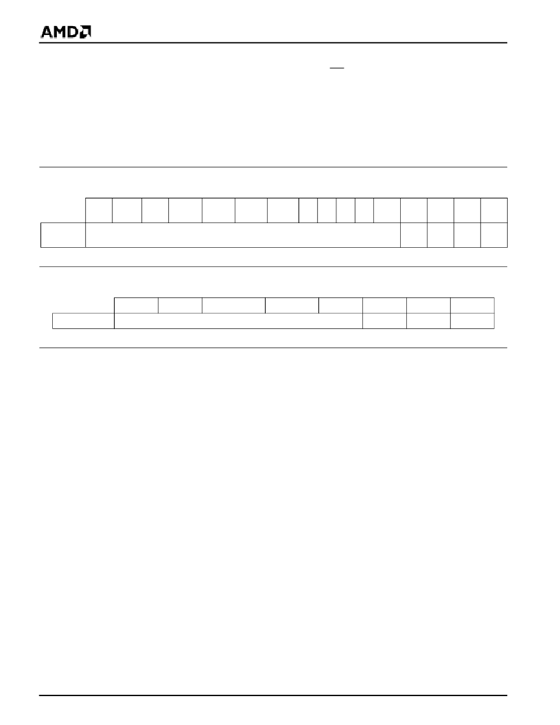
Table 10. Test Register (TR4)
31
30–29
28
27–26
25–24
23–22
21–20
19
18
17
16
15–
11
10
9–7
6–3
2–0
EXT = 0
Tag
Valid
LRU
Valid
(rd)
Not
used
Table 11. Test Register (TR5)
31–20
19
18–17
16
15–11
10–4
3–2
1–0
Write-Through
Not used
Index
Entry
Control
相關(guān)PDF資料 |
PDF描述 |
|---|---|
| AM486DX | Am486DX - Am486DX Block Diagram |
| AM486DXPGA | Am486DX PGA - Am486DX PGA Package Temperature Comparisons |
| AM486DXSQFP | 70NS, PLCC, IND TEMP(EEPROM) |
| AM486 | Am486 Microprocessor Software User's Manual? 4.40MB (PDF) |
| AM49DL3208G | Am49DL3208G - Stacked Multi-Chip Package (MCP) Flash Memory and pSRAM |
相關(guān)代理商/技術(shù)參數(shù) |
參數(shù)描述 |
|---|---|
| AM486DE2-66V8TGC | 制造商:AMD 制造商全稱:Advanced Micro Devices 功能描述:8-Kbyte Write-Through Embedded Microprocessor |
| AM486DE2-66V8THC | 制造商:Advanced Micro Devices 功能描述:Microprocessor, 32 Bit, 208 Pin, Plastic, QFP |
| AM486DX | 制造商:未知廠家 制造商全稱:未知廠家 功能描述:Am486DX - Am486DX Block Diagram |
| AM486DX/DX2 | 制造商:未知廠家 制造商全稱:未知廠家 功能描述:Am486DX/DX2 Hardware Reference Manual |
| AM486DX2 | 制造商:AMD 制造商全稱:Advanced Micro Devices 功能描述:Am5X86⑩ Microprocessor Family |
發(fā)布緊急采購,3分鐘左右您將得到回復(fù)。