- 您現(xiàn)在的位置:買(mǎi)賣(mài)IC網(wǎng) > PDF目錄362278 > AM486DXPGA Am486DX PGA - Am486DX PGA Package Temperature Comparisons PDF資料下載
參數(shù)資料
| 型號(hào): | AM486DXPGA |
| 英文描述: | Am486DX PGA - Am486DX PGA Package Temperature Comparisons |
| 中文描述: | Am486DX美巡賽- Am486DX PGA封裝溫度比較 |
| 文件頁(yè)數(shù): | 31/52頁(yè) |
| 文件大小: | 1242K |
| 代理商: | AM486DXPGA |
第1頁(yè)第2頁(yè)第3頁(yè)第4頁(yè)第5頁(yè)第6頁(yè)第7頁(yè)第8頁(yè)第9頁(yè)第10頁(yè)第11頁(yè)第12頁(yè)第13頁(yè)第14頁(yè)第15頁(yè)第16頁(yè)第17頁(yè)第18頁(yè)第19頁(yè)第20頁(yè)第21頁(yè)第22頁(yè)第23頁(yè)第24頁(yè)第25頁(yè)第26頁(yè)第27頁(yè)第28頁(yè)第29頁(yè)第30頁(yè)當(dāng)前第31頁(yè)第32頁(yè)第33頁(yè)第34頁(yè)第35頁(yè)第36頁(yè)第37頁(yè)第38頁(yè)第39頁(yè)第40頁(yè)第41頁(yè)第42頁(yè)第43頁(yè)第44頁(yè)第45頁(yè)第46頁(yè)第47頁(yè)第48頁(yè)第49頁(yè)第50頁(yè)第51頁(yè)第52頁(yè)
Am486DE2 Microprocessor
31
Bit 0 indicates whether the opcode that was accessing
the I/O location was performing either a read (1) or a
write (0) operation as indicated by the R/W bit.
If an SMI occurs and it does not trap an I/O instruction,
the contents of the I/O address and R/W bit are unpre-
dictable and should not be used.
SMM Base Relocation
The Am486DE2 processor provides a control register
not in the standard Am486DX processor: SMBASE. The
SMRAM address space can be modified by changing
the SMBASE register before exiting an SMI handler rou-
tine. SMBASE can be changed to any 32K-aligned val-
ue. (Values that are not 32K-aligned cause the CPU to
enter the Shutdown state when executing the RSM in-
struction.) SMBASE is set to the default value of 30000h
on RESET. If SMBASE is changed by an SMI handler,
all subsequent SMI requests initiate a state save at the
new SMBASE.
The SMBASE slot in the SMM state-save area indicates
and changes the SMI jump-vector location and SMRAM-
save area. When bit 17 of the SMM Revision Identifier
is set, then this feature exists and the SMRAM base and
consequently, the jump vector, are as indicated by the
SMM Base slot (see Table 7). During the execution of
the RSM instruction, the CPU reads this slot and initial-
izes the CPU to use the new SMBASE during the next
SMI. During an SMI, the CPU does its context save to
the new SMRAM area pointed to by the SMBASE, stores
the current SMBASE in the SMM Base slot (offset
7EF8h), and then starts execution of the new jump vec-
tor based on the current SMBASE (see Figure 12).
The SMBASE must be a 32-Kbyte aligned, 32-bit integer
that indicates a base address for the SMRAM context
save area and the SMI jump vector. For example, when
the processor first powers up, the minimum SMRAM
area is from 38000h–3FFFFh. The default SMBASE is
30000h.
As illustrated in Figure 13, the starting address of the
jump vector is calculated by:
SMBASE + 8000h
The starting address for the SMRAM state-save area is
calculated by:
SMBASE + [8000h + 7FFFh]
When this feature is enabled, the SMRAM register map
is addressed according to the above formula.
To change the SMRAM base address and SMI jump
vector location, the SMI handler modifies the SMBASE
slot. Upon executing an RSM instruction, the processor
reads the SMBASE slot and stores it internally. Upon
recognition of the next SMI request, the processor uses
the new SMBASE slot for the SMRAM dump and SMI
jump vector. If the modified SMBASE slot does not con-
tain a 32-Kbyte aligned value, the RSM microcode caus-
es the CPU to enter the Shutdown state.
SMM System Design Considerations
SMRAM Interface
The hardware designed to control the SMRAM space
must follow these guidelines:
I
Initialize SMRAM space during system boot up.
Initialization must occur before the first SMI occurs.
Initialization of SMRAM space must include installation
of an SMI handler and may include installation of
related data structures necessary for particular SMM
applications. The memory controller interfacing
SMRAM should provide a means for the initialization
code to open the SMRAM space manually.
I
The memory controller must decode a minimum
initial SMRAM address space of 38000h–3FFFFh.
I
Alternate bus masters (such as DMA controllers)
must not be able to access SMRAM space. The
system should allow only the CPU, either through
SMI or during initialization, to access SMRAM.
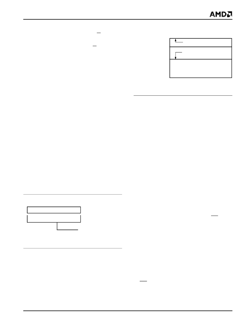
Figure 12. SMM Base Slot Offset
31
0
SMM Base
Register Offset 7EF8h
Figure 13. SRAM Usage
SMI Handler Entry Point
SMBASE + 8000h
+ 7FFFh
SMRAM
SMBASE + 8000h
SMBASE
Start of State Save
相關(guān)PDF資料 |
PDF描述 |
|---|---|
| AM486DXSQFP | 70NS, PLCC, IND TEMP(EEPROM) |
| AM486 | Am486 Microprocessor Software User's Manual? 4.40MB (PDF) |
| AM49DL3208G | Am49DL3208G - Stacked Multi-Chip Package (MCP) Flash Memory and pSRAM |
| AM49DL320BG | Am49DL320BG - Stacked Multi-Chip Package (MCP) Flash Memory and SRAM |
| AM49DL32XBG | Am49DL32xBG - Stacked Multi-Chip Package (MCP) Flash Memory and SRAM |
相關(guān)代理商/技術(shù)參數(shù) |
參數(shù)描述 |
|---|---|
| AM486DXSQFP | 制造商:未知廠家 制造商全稱(chēng):未知廠家 功能描述:Am486DX SQFP - Am486DX SQFP Package Temperature Comparisons |
| AM486-EVAL-KIT | 制造商:Advanced Micro Devices 功能描述:AM486CDP EVAL KIT |
| AM4874N | 制造商:ANALOGPOWER 制造商全稱(chēng):ANALOGPOWER 功能描述:N-Channel 30-V (D-S) MOSFET |
| AM4890N | 制造商:ANALOGPOWER 制造商全稱(chēng):ANALOGPOWER 功能描述:Dual N-Channel 150-V (D-S) MOSFET |
| AM4892N | 制造商:ANALOGPOWER 制造商全稱(chēng):ANALOGPOWER 功能描述:Dual N-Channel 150-V (D-S) MOSFET |
發(fā)布緊急采購(gòu),3分鐘左右您將得到回復(fù)。