- 您現(xiàn)在的位置:買賣IC網(wǎng) > PDF目錄362330 > AN-35 LinkSwitch Design Guide PDF資料下載
參數(shù)資料
| 型號: | AN-35 |
| 英文描述: | LinkSwitch Design Guide |
| 中文描述: | 使用LinkSwitch設(shè)計(jì)指南 |
| 文件頁數(shù): | 4/16頁 |
| 文件大小: | 504K |
| 代理商: | AN-35 |
AN-35
4
B
4/03
the sum of actual output power P
and the following loss terms:
cable power P
, diode power P
, bias power P
(the
power required to drive the
LinkSwitch
CONTROL pin),
transformer secondary copper loss P
S(CU)
, and transformer core
loss P
CORE
.
=
=
=
K
CORE
=
R
is the total cable DC resistance, I
is the nominal CC
output current, V
is output diode forward voltage drop, V
is reflected output voltage, I
is secondary RMS current,
R
is output winding DC resistance, V
is core effective
volume and K
is core loss per unit volume. As before, if no
better estimates or measurements are available, use 0.15
for
R
, 0.7 V for the forward voltage (V
DOUT
) of a Schottky diode
or 1.1 V for a PN diode, 0.3
for R
and I
equal to
4
x
I
. Both V
and K
can be read from the ferrite core
manufacturer
’
s material curves. To find K
, use the core flux
swing B
. In discontinuous mode operation, AC Flux Density
B
AC
is equal to B
M
:
The next transformer design step is to calculate the nominal
primary inductance L
. L
tolerance should be within
±
10% (to
meet peak power CC tolerance of
±
20% for LNK501,
±
25% for
LNK500). The simple
LinkSwitch
feedback circuit is designed
specifically for discontinuous mode operation. Continuous
mode designs result in control loop instability and are therefore
not recommended. For proper CC operation, the
LinkSwitch
transformer must therefore be designed for discontinuous
operation under all line/load conditions.
At the peak power point, the power processed by the core or
P
O(EFF)
is given by:
L
P
is the nominal transformer primary inductance, I
is equal to
the
LinkSwitch
parameter I
and f
is the switching frequency.
Note that I
and f
are enclosed in brackets as the
LinkSwitch
data
sheet specifies an I
2
f coefficient equal to the I
2
f
normalized to I
. By normalizing to I
(the CONTROL pin
current at 30% duty cycle), the effect of I
tolerance is
included and does not need to be considered separately. Output
power is therefore dependent primarily on transformer primary
inductance tolerance (typically
±
10% for low cost high volume
production methods).
As shown above, effective output power P
is calculated
from the total energy stored in the transformer and is therefore
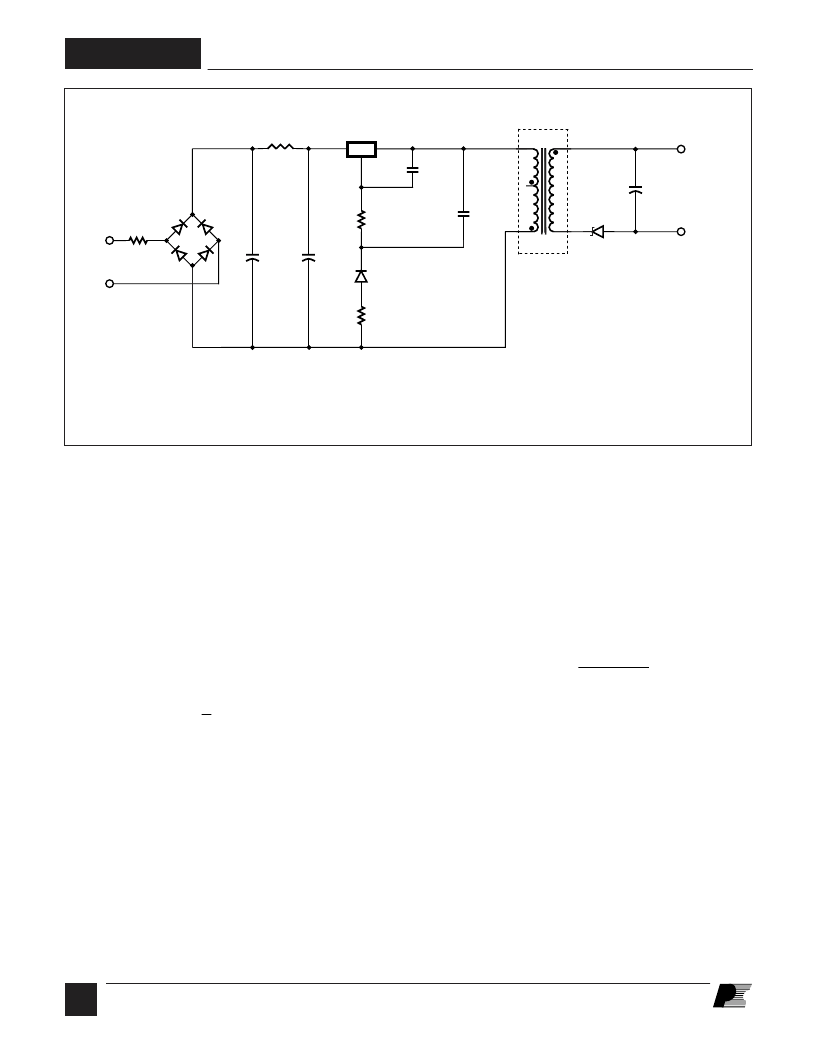
Figure 3. Example Schematic for a Typical LinkSwitch Charger.
(12)
P
L
I
f
O EFF
(
P
P
S
)
=
×
×
×
[
]
1
2
2
(6)
(10)
(11)
(7)
(8)
(9)
B
B
AC
M
=
P
P
P
R
V
I
I
V
mA
V
E
CABLE
CABLE
O
DIODE
DOUT
×
O
BIAS
OR
×
×
2
2 3
P
P
I
R
CORE
S CU
(
SEC RMS
(
SEC
×
=
×
2
2
)
)
C1
4.7
μ
F
400 V
C2
4.7
μ
F
400 V
RF1
10
1 W
Fusible
L1
1 mH
R1
20.5 k
1%
R2
100
D5
1N4937
C4
0.1
μ
F
100 V
116 T
#34 AWG
EE13
L
P
= 2.55 mH
15 T
#30 AWG
TIW
3
4
1
5
T1
6
D6
11DQ06
C5
470
μ
F
10 V
85-265
VAC
U1
LinkSwitch
D
5.5 V,
500 mA
RTN
BR1
1 A, 600 V
PI-3476-032403
PERFORMANCE SUMMARY
Output Power:
Efficiency:
No Load
Consumption:
2.75 W
≥
72%
260 mW, 230 VAC
200 mW, 115 VAC
C3
0.22
μ
F
50 V
S
C
相關(guān)PDF資料 |
PDF描述 |
|---|---|
| AN002M4-78 | SP4T RF Absorptive Switch |
| AN002R2-29 | SPDT RF Reflective Switch |
| AN002R2-53 | SPDT RF Reflective Switch |
| AN1081 | Voltage-Feedback Operational Amplifier |
| AN1081S | Voltage-Feedback Operational Amplifier |
相關(guān)代理商/技術(shù)參數(shù) |
參數(shù)描述 |
|---|---|
| AN3500-521P | 制造商:未知廠家 制造商全稱:未知廠家 功能描述:AN0625-521P |
| AN3501FBP | 制造商:Panasonic Industrial Company 功能描述:IC |
| AN3501NFBP | 制造商:PANASONIC 制造商全稱:Panasonic Semiconductor 功能描述:Luminance, chroma and linear audio signal processing IC for VCR |
| AN350-4 | 制造商:AN# - MILITARY 功能描述: |
| AN3-52A | 制造商:AN# - MILITARY 功能描述: |
發(fā)布緊急采購,3分鐘左右您將得到回復(fù)。