- 您現(xiàn)在的位置:買賣IC網(wǎng) > PDF目錄378405 > AND8112 (ON SEMICONDUCTOR) A Quasi-Resonant SPICE Model Eases Feedback Loop Designs PDF資料下載
參數(shù)資料
| 型號: | AND8112 |
| 廠商: | ON SEMICONDUCTOR |
| 英文描述: | A Quasi-Resonant SPICE Model Eases Feedback Loop Designs |
| 中文描述: | 阿準諧振SPICE模型反饋環(huán)的設(shè)計更易 |
| 文件頁數(shù): | 5/12頁 |
| 文件大小: | 205K |
| 代理商: | AND8112 |
AND8112/D
http://onsemi.com
5
1
2
3
4
5
8
7
6
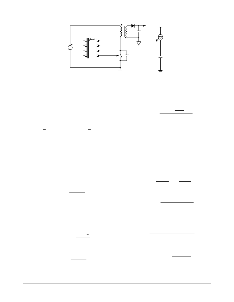
NCP1207
V
D1
Figure 8.
V
g
C
tot
C
tot
V
g
C
out
<=>
When the power switch turns off, the primary inductor behaves like a current source that charges the C
tot
capacitor. This sequence ends
when voltage developed across C
tot
exceeds [V
g
+(V+V
f
)/N], that is when the secondary diode D1 starts to conduct.
+
2. At the end of the core reset, both switches (power
switch and secondary diode) are off. The primary
inductor L
P
together with C
tot
form a LC network.
C
tot
voltage (and thus the drain source voltage of
the power switch) oscillates around the input
voltage V
g
between a peak value (the initial level:
Vg
N
) and a valley value
Vg
effects being neglected. To benefit from the quasi
resonant mode, it is recommended to turn the power
switch on in the valley, where the drainsource
voltage is minimized. This naturally reduces the
dV/dt and switching losses to a minimum (in
practice, an appropriate delay inserted after the core
reset detection provides an effective method to
synchronize the power switch turn on with the valley
event). A simple look at Figure 7 shows that the
valley occurs at half the oscillation period.
Therefore, the delay
completion and the optimal turn on time is given by
the following equation:
LP
Once these delays are defined, it is about time to revise the
previous equations in order to include
The main parameters of interest are the average input and
output currents, the equivalent resistance and the switching
period. If we combine equations 24 and 13 that express I
P
as
a function of the input voltage, the inductor value and the
ONtime leads to:
V
V
the damping
t2
between the core reset
t2
Ctot
(eq. 25)
t1
and
t2
effects.
t1
LP
Ctot
Vg
Vg
V
N
ton
(eq. 26)
If (d
′
x T
S
) depicts the core reset time,
require to change (d
′
=1d) into:
t1
and
t2
times
d
1
d
t1
t2
TS
(eq. 27)
The inductor voltsecond balance approximation of
equation 8 still holds. However, it must be revised by
replacing d
′
(t) by its novel value as expressed by
equation (27):
1
V(LP)
d
Vg
d
t1
t2
TS
V
N
0
(eq. 28)
Rearranging equation (28), one can unveil the duty cycle
expression:
1
TS
(N
Vg)
The switching period is the sum of the ontime, the core
reset time (t
demag
),
t1
and
t2
:
TS
ton
tdemag
The time t
demag
can be easily deducted from the Figure 4
sketch. Since the core reset is the time necessary to discharge
the primary inductor from I
P
to zero with a (V+V
f
)/N slope,
it comes:
d
t1
t2
V
V
(eq. 29)
t1
t2
(eq. 30)
tdemag
LP
IP
V N
ton
N
Vg
V
(eq. 31)
Substitution of equation (31) into (eq. 30), leads to the
following expression where T
S
is a function of
t
on
:
[(N
TS
t1
t2
Vg)
V]
ton
N
(eq. 32)
Equation (15) that defines the average input current as a
function of the input voltage, the duty cycle, the inductor
value and the switching period, still holds. Substitution of
equation (29) into equation (15) leads to:
I1(t)
Vg
1
LP
t1
t2
TS
V
ton
V]
2
[(N
Vg)
(eq. 33)
Replacing T
S
by its equation 32 expression, it comes:
I1(t)
Vg
1
t1
t2
t1
t2
(N
Vg)
V
ton
V
V
ton
2
LP
[(N
Vg)
V]
(eq. 34)
Rearranging this equation, one can obtain:
相關(guān)PDF資料 |
PDF描述 |
|---|---|
| AND8116 | Integrated Relay/Inductive Load Drivers for Industrial and Automotive Applications |
| AND8116D | Integrated Relay/Inductive Load Drivers for Industrial and Automotive Applications |
| AND8130 | Analog Switch Allows USB Switching at Low Voltages |
| AND8139 | Ultra-Low Voltage MiniGate Devices Solve 1.2 V Interface Problems |
| AND8139D | Ultra-Low Voltage MiniGate Devices Solve 1.2 V Interface Problems |
相關(guān)代理商/技術(shù)參數(shù) |
參數(shù)描述 |
|---|---|
| AND8116 | 制造商:ONSEMI 制造商全稱:ON Semiconductor 功能描述:Integrated Relay/Inductive Load Drivers for Industrial and Automotive Applications |
| AND8116D | 制造商:ONSEMI 制造商全稱:ON Semiconductor 功能描述:Integrated Relay/Inductive Load Drivers for Industrial and Automotive Applications |
| AND8130 | 制造商:ONSEMI 制造商全稱:ON Semiconductor 功能描述:Analog Switch Allows USB Switching at Low Voltages |
| AND8130/D | 制造商:ONSEMI 制造商全稱:ON Semiconductor 功能描述:Analog Switch Allows USB Switching at Low Voltages |
| AND8139 | 制造商:ONSEMI 制造商全稱:ON Semiconductor 功能描述:Ultra-Low Voltage MiniGate Devices Solve 1.2 V Interface Problems |
發(fā)布緊急采購,3分鐘左右您將得到回復(fù)。