- 您現(xiàn)在的位置:買(mǎi)賣(mài)IC網(wǎng) > PDF目錄378405 > AND8112 (ON SEMICONDUCTOR) A Quasi-Resonant SPICE Model Eases Feedback Loop Designs PDF資料下載
參數(shù)資料
| 型號(hào): | AND8112 |
| 廠商: | ON SEMICONDUCTOR |
| 英文描述: | A Quasi-Resonant SPICE Model Eases Feedback Loop Designs |
| 中文描述: | 阿準(zhǔn)諧振SPICE模型反饋環(huán)的設(shè)計(jì)更易 |
| 文件頁(yè)數(shù): | 8/12頁(yè) |
| 文件大小: | 205K |
| 代理商: | AND8112 |
AND8112/D
http://onsemi.com
8
7
BEt
Voltage
(2*{Lp}*(V(3)+{N}*V(13))/(V(ton)*V(3)+1u))*I(V6)
1
VI1
1
4
4
3
3
BGd
Current
(((2*{Lp}*(V(3)+{N}*V(13))/(V(ton)*V(3)+1u))*I(V6)^2)/(V(3,4)+1u))*{eff}
FB
Bton
Voltage
V(errint)*{Lp}/({Rs}*V(13))
12
Rs
{Rlf}
13
X2
XFMR
RATIO = N
Lm
{Lp}
1
4
R9
1 Meg
BIp
Voltage
V(ton)*V(13)/{Lp}
BToff
Voltage
{Lp}*V(Ip)*{N}/V(3)
Bfreq
Voltage
(1/(V(ton)+V(toff)))/1 k
20
Bclamp
Current
I(VI1)>0
I(VI1) :
0
V6
System Parameter calculation
t
off
Operating Parameter Calculation
B8
Voltage
V(FB)/3 > 1 1 : V(FB)/3 < 10 m
10m : V(FB)/3
errint
13
Gnd
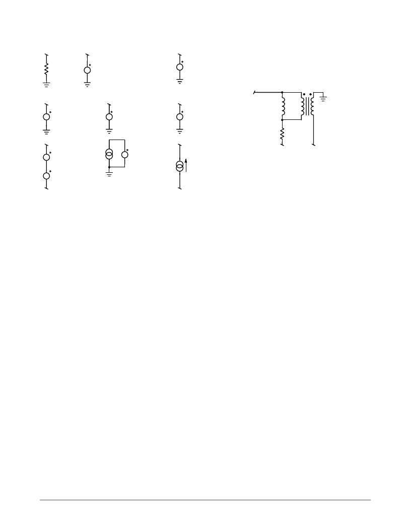
Figure 10. The final simplified model implementation where added sources reveal operating parameters
such as T
on
, F
SW
and the peak current I
P
Figure 10 portrays the final simplified model subcircuit where all relevant sources appear, among them, the switching
frequency, peak current and T
on
calculations. For the extended model, only BGd and BEt sources need to be changed. As you
can see, there are plenty denominator expressions where a variable such as T
on
appears. If during the bias point calculation
SPICE T
on
starts or goes close to zero, the simulator can fail to converge (or find a wrong bias point which is worse). To avoid
this potential problem, a trick consists in inserting a fixed value, small enough like 1 or less, to clamp the maximum value
the source can take if T
on
becomes null. To the opposite, the frequency expression modeled by a voltage source can deliver
kV to express kilo Hz. The simulator dynamic being bounded, mixing values of a few mV with sources delivering kV can puzzle
the bias point calculation. Again, a division by 1000 will limit the range. The FB pin undergoes a division by 3 to be further
clamp by a 1 V limiter, a classical circuitry found in most PWM controllers (I
P
max = 1 V / R
sense
).
DCbias calculation always represents a difficult task for SPICE simulators running averaged models. In order to enhance
the extended model robustness (the one including parasitic effects), we have constrained the BGd source to be positive only
by using a simple inline equation that differs depending on the simulator syntax:
IsSpice
BGd 4 3 I= ((2*{Lp}/V(ton)) * ( ({N}*V(13)+V(3))/(V(3)+1u) + {DEL}/V(ton) +
+({Lp}*{Ctot}/V(ton))*(1+(V(3)/{N})/V(13)) ) * I(V6)^2)/(V(3,4)+1u)*{EFF} < 10m 10m :
+((2*{Lp}/V(ton)) * ( ({N}*V(13)+V(3))/(V(3)+1u) + {DEL}/V(ton) +
+({Lp}*{Ctot}/V(ton))*(1+(V(3)/{N})/V(13)) ) * I(V6)^2)/(V(3,4)+1u)*{EFF}
PSpice
Gd 4 3 TABLE { ((2*{Lp}/(V(ton)+10n)) * ( ({N}*V(13)+V(3))/(V(3)+1u) + {DEL}/(V(ton)+10n) +
+({Lp}*{Ctot}/(V(ton)+10 n))*(1+(V(3)/{N})/V(13)) )
+ * I(V6)^2)/(V(3,4) + 1u)*{EFF} } ( (10m,10m) (1000,1000) )
Finally, the model comes with two different names:
.SUBCKT QuasiFly 13 FB GND 3 I
P
T
on
F
SW
params: L
P
= 3.22 m R
S
= 0.5 N = 0.06 eff = 0.86
the simplified model version
QuasiFlyDel 13 FB GND 3 I
P
T
on
F
SW
params: L
P
= 3.22 m R
S
= 0.8 N = 0.06 eff = 0.86 C
tot
= 100 p
the complete model including parasitic effects
Passed parameters are:
C
tot
, the lump parasitic component present on the drain.
L
P
, the primary inductance
R
lf
, the ohmic losses of the primary winding
N, the N
P
: N
S
ratio with N
P
=1
Eff, the circuit estimated efficiency
Please note that for the sake of simplicity, both models do not account for the secondary rectifier forward drop V
f
whose effect
is nevertheless negligible in our approach.
t
on
F
SW
I
P
相關(guān)PDF資料 |
PDF描述 |
|---|---|
| AND8116 | Integrated Relay/Inductive Load Drivers for Industrial and Automotive Applications |
| AND8116D | Integrated Relay/Inductive Load Drivers for Industrial and Automotive Applications |
| AND8130 | Analog Switch Allows USB Switching at Low Voltages |
| AND8139 | Ultra-Low Voltage MiniGate Devices Solve 1.2 V Interface Problems |
| AND8139D | Ultra-Low Voltage MiniGate Devices Solve 1.2 V Interface Problems |
相關(guān)代理商/技術(shù)參數(shù) |
參數(shù)描述 |
|---|---|
| AND8116 | 制造商:ONSEMI 制造商全稱(chēng):ON Semiconductor 功能描述:Integrated Relay/Inductive Load Drivers for Industrial and Automotive Applications |
| AND8116D | 制造商:ONSEMI 制造商全稱(chēng):ON Semiconductor 功能描述:Integrated Relay/Inductive Load Drivers for Industrial and Automotive Applications |
| AND8130 | 制造商:ONSEMI 制造商全稱(chēng):ON Semiconductor 功能描述:Analog Switch Allows USB Switching at Low Voltages |
| AND8130/D | 制造商:ONSEMI 制造商全稱(chēng):ON Semiconductor 功能描述:Analog Switch Allows USB Switching at Low Voltages |
| AND8139 | 制造商:ONSEMI 制造商全稱(chēng):ON Semiconductor 功能描述:Ultra-Low Voltage MiniGate Devices Solve 1.2 V Interface Problems |
發(fā)布緊急采購(gòu),3分鐘左右您將得到回復(fù)。