- 您現(xiàn)在的位置:買賣IC網(wǎng) > PDF目錄362374 > APC08Y08-W Non-Isolated DC/DC Power Module PDF資料下載
參數(shù)資料
| 型號(hào): | APC08Y08-W |
| 英文描述: | Non-Isolated DC/DC Power Module |
| 中文描述: | 非隔離DC / DC電源模塊 |
| 文件頁數(shù): | 8/23頁 |
| 文件大小: | 2632K |
| 代理商: | APC08Y08-W |
Technical Reference Note (APC08)
MODEL: APC08 SERIES
OCTOBER 4, 2004 - REVISION 03
SHEET 8 OF 23
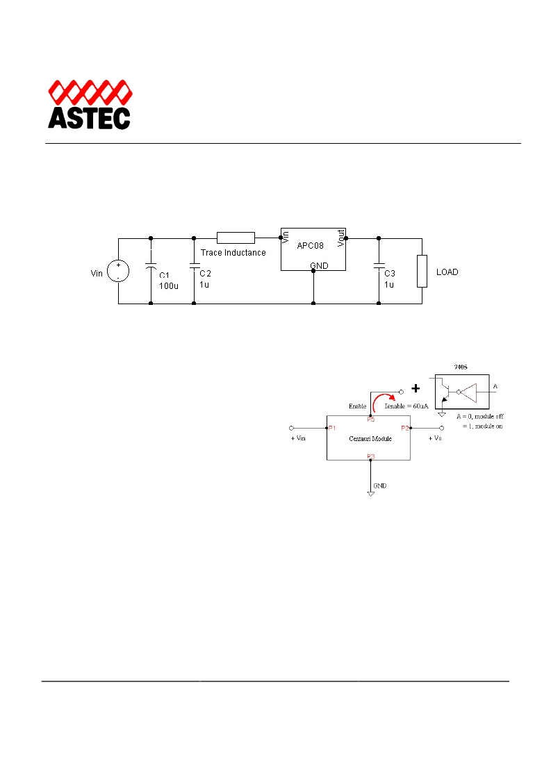
Typical Application Circuit (Standard Pinout)
Recommended C1 is a low ESR (<100 mohms) 100 μF tantalum and C2 is a 1 μF ceramic or equivalent. Recommended
output decoupling capacitor C3 for –W models is 22 μF low ESR ceramic capacitor (at a min). For all other models, C3 can go
as low as 1 μF ceramic capacitor.
Figure 2. Typical Application Circuit.
Enable Pin (Standard configuration)
Pin P5 is functioned to enable the output voltage of a
module. If this pin is left open or connected to > 4.1Vdc
up to 14Vdc, the module is turned on. On the other hand,
if this pin is connected to ground or to a voltage potential
from 0 to 0.8Vdc, the module is turned off. The enable pin
can source current up to 60
μ
A max - suited for typical
open-collector transistors readily available in the market.
For TTL compatibility, Figure 3 shows a 7405 open
collector inverter IC utilized to function the Enable
feature. Other common chips that can do the function are
74S05; 74HCT05; non-inverting - 7407; 74S07; 74HC07.
If SMT packaging is preferred, Fairchild's Tiny Logic
NC7SZ05 or TI's Little Logic SN7SLVC1G06 comes in SOT23
or SC70 packages.
Special Feature Pins (Options):
Trim Function (-9):
Pin P4 is used for output voltage adjustment. The output voltage can be trimmed through an external resistor or through an
external DC supply as described in the succeeding sections.
Method 1: External Trim Resistor
.
By connecting an external resistor across P4 and P3 (Gnd), the voltage appearing on pin P2 (Vo) is adjusted to a higher value.
The output voltage of a module can be adjusted up to a maximum value of 3.3V (nominal) or 83% of the input voltage,
Figure 3. Output Voltage Enable function diagram.
相關(guān)PDF資料 |
PDF描述 |
|---|---|
| APC12M08 | 40 Watts |
| APC12 | 40 Watts |
| APC12F03 | 40 Watts |
| APC12F08 | 40 Watts |
| APC12G03 | 40 Watts |
相關(guān)代理商/技術(shù)參數(shù) |
參數(shù)描述 |
|---|---|
| APC1 | 制造商:LUMINIS 制造商全稱:LUMINIS 功能描述:Attachment accessories |
| APC100SS | 功能描述:TOOL 制造商:astro tool corp 系列:- 零件狀態(tài):有效 工具類型:- 配套使用產(chǎn)品/相關(guān)產(chǎn)品:- 特性:- 標(biāo)準(zhǔn)包裝:1 |
| APC103 | 功能描述:TOOL 制造商:astro tool corp 系列:- 零件狀態(tài):有效 工具類型:- 配套使用產(chǎn)品/相關(guān)產(chǎn)品:- 特性:- 標(biāo)準(zhǔn)包裝:1 |
| APC103D/Z | 制造商:Assmann Electronics Inc 功能描述: |
| APC106 | 功能描述:TOOL 制造商:astro tool corp 系列:- 零件狀態(tài):有效 工具類型:- 配套使用產(chǎn)品/相關(guān)產(chǎn)品:- 特性:- 標(biāo)準(zhǔn)包裝:1 |
發(fā)布緊急采購,3分鐘左右您將得到回復(fù)。