- 您現(xiàn)在的位置:買(mǎi)賣(mài)IC網(wǎng) > PDF目錄362444 > AS5C4008DJECJ-15 x8 SRAM PDF資料下載
參數(shù)資料
| 型號(hào): | AS5C4008DJECJ-15 |
| 英文描述: | x8 SRAM |
| 中文描述: | x8的SRAM |
| 文件頁(yè)數(shù): | 3/12頁(yè) |
| 文件大小: | 136K |
| 代理商: | AS5C4008DJECJ-15 |
S R A M
AS5C4009
Austin Semiconductor, Inc.
AS5C4009
Rev. 5.0 6/03
Austin Semiconductor, Inc. reserves the right to change products or specifications without notice.
3
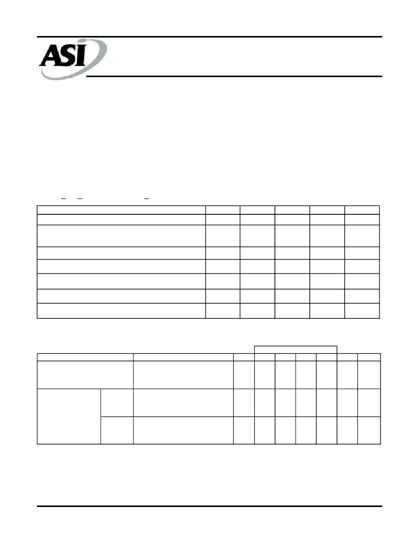
ABSOLUTE MAXIMUM RATINGS*
Voltage on Vcc Supply Relative to Vss...................-.5V to +7.0V
Voltage on any pin Relative to Vss..........................-.5V to +7.0V
Storage Temperature ....................................-65
°
C to +150
°
C
Operating Temperature Range.............................-55
o
C to +125
o
C
Soldering Temperature Range...............................................260
o
C
Maximum Junction Temperature**....................................+150
°
C
Power Dissipation...................................................................1.0W
*Stresses greater than those listed under "Absolute Maximum
Ratings" may cause permanent damage to the device. This is
a stress rating only and functional operation of the device at
these or any other conditions above those indicated in the
operation section of this specification is not implied. Exposure
to absolute maximum rating conditions for extended periods
may affect reliability.
** Junction temperature depends upon package type, cycle
time, loading, ambient temperature and airflow.
ELECTRICAL CHARACTERISTICS AND RECOMMENDED DC OPERATING CONDITIONS
(-55
o
C < T
A
< 125
o
C; Vcc = 5V +10%)
PARAMETER/CONDITION
Input Leakage Current (V
IN
= V
SS
to V
CC
)
Output Leakage Current
(CE\=V
IH
or OE\=V
IH
or WE\=V
IL
, V
IO
=V
SS
to V
CC
)
MIN
-5
MAX
5
UNITS
μΑ
NOTES
-5
5
μΑ
Output Low Voltage (I
OL
= 2.1mA)
--
0.4
V
15
Output High Voltage (I
OH
= -1.0 mA)
2.4
--
V
15
Supply Voltage
4.5
5.5
V
15
Input High (Logic 1) Voltage
2.2
Vcc +0.5
V
1, 15
Input Low (Logic 0) Voltage
-0.5
0.8
V
2, 15
V
IL
SYMBOL
I
LI
I
LO
V
OL
V
OH
V
CC
V
IH
CONDITIONS
Cycle Time = Min., 100%
Duty Cycle, I
IO
= 0mA,
CE\ = V
IL
, V
IN
= V
IH
or V
IL
SYM
-55
-70
-85
-100
UNITS NOTES
I
cc1
100
90
80
70
mA
3
TTL
CE\ = V
IH
,
Other inputs = V
IL
or V
IH
I
SB
6
6
6
6
mA
CMOS
CE\ = Vcc -0.2V,
Other inputs = 0 ~ Vcc
I
SB1
0.75
0.75
0.75
0.75
mA
MAX
Power Supply Current:
Operating
PARAMETER
Power Supply Current:
Standby
相關(guān)PDF資料 |
PDF描述 |
|---|---|
| AS5C4008DJECJ-17 | x8 SRAM |
| AS5C4008DJECJ-20 | x8 SRAM |
| AS5C512K8DJECJ-12 | x8 SRAM |
| AS5C512K8DJECJ-15 | x8 SRAM |
| AS5C512K8DJECJ-17 | x8 SRAM |
相關(guān)代理商/技術(shù)參數(shù) |
參數(shù)描述 |
|---|---|
| AS5C4008DJECJ-17 | 制造商:未知廠(chǎng)家 制造商全稱(chēng):未知廠(chǎng)家 功能描述:x8 SRAM |
| AS5C4008DJECJ-20 | 制造商:未知廠(chǎng)家 制造商全稱(chēng):未知廠(chǎng)家 功能描述:x8 SRAM |
| AS5C4008EC-12/883C | 制造商:Micross Components, Inc. 功能描述:SRAM, 4MB - Trays |
| AS5C4008EC-12/H | 制造商:AUSTIN 制造商全稱(chēng):Austin Semiconductor 功能描述:512K x 8 SRAM SRAM MEMORY ARRAY |
| AS5C4008EC-12/IT | 制造商:Micross Components 功能描述:SRAM, 4MB - Trays |
發(fā)布緊急采購(gòu),3分鐘左右您將得到回復(fù)。