- 您現(xiàn)在的位置:買賣IC網(wǎng) > PDF目錄166232 > AS5SS256K36ADQ-8.5/883C (AUSTIN SEMICONDUCTOR INC) 256K x 36 SSRAM Flow-Through, Synchronous Burst SRAM PDF資料下載
參數(shù)資料
| 型號: | AS5SS256K36ADQ-8.5/883C |
| 廠商: | AUSTIN SEMICONDUCTOR INC |
| 元件分類: | SRAM |
| 英文描述: | 256K x 36 SSRAM Flow-Through, Synchronous Burst SRAM |
| 中文描述: | 256K X 36 STANDARD SRAM, 8.5 ns, PQFP100 |
| 封裝: | 14 X 20 MM, 1.40 MM HEIGHT, MS-026, TQFP-100 |
| 文件頁數(shù): | 13/16頁 |
| 文件大小: | 391K |
| 代理商: | AS5SS256K36ADQ-8.5/883C |
SSRAM
AS5SS256K36 &
AS5SS256K36A
AS5SS256K36 &
AS5SS256K36A
Rev. 3.6 06/05
Austin Semiconductor, Inc. reserves the right to change products or specifications without notice.
6
Austin Semiconductor, Inc.
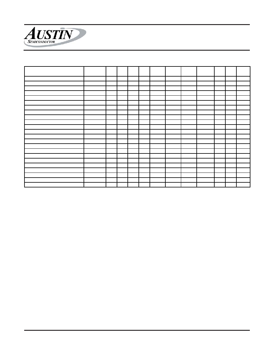
TRUTH TABLE
OPERATION
ADDRESS
USED
CE\ CE2\ CE2
ZZ
ADSP\
ADSC\
ADV\
WRITE\
OE\ CLK
DQ
Deselected Cycle, Power-Down
None
H
X
L
X
L
X
L-H High-Z
Deselected Cycle, Power-Down
None
L
X
L
X
L-H High-Z
Deselected Cycle, Power-Down
None
L
H
X
L
X
L-H High-Z
Deselected Cycle, Power-Down
None
L
X
L
H
L
X
L-H High-Z
Deselected Cycle, Power-Down
None
L
H
X
L
H
L
X
L-H High-Z
SNOOZE MODE, Power-Down
None
X
H
X
High-Z
READ Cycle, Begin Burst
External
L
H
L
X
L
L-H
Q
READ Cycle, Begin Burst
External
L
H
L
X
H
L-H High-Z
WRITE Cycle, Begin Burst
External
L
H
L
H
L
X
L
X
L-H
D
READ Cycle, Begin Burst
External
L
H
L
H
L
X
H
L
L-H
Q
READ Cycle, Begin Burst
External
L
H
L
H
L
X
H
L-H High-Z
READ Cycle, Continue Burst
Next
X
L
H
L
H
L
L-H
Q
READ Cycle, Continue Burst
Next
X
L
H
L
H
L-H High-Z
READ Cycle, Continue Burst
Next
H
X
L
X
H
L
H
L
L-H
Q
READ Cycle, Continue Burst
Next
H
X
L
X
H
L
H
L-H High-Z
WRITE Cycle, Continue Burst
Next
X
L
H
L
X
L-H
D
WRITE Cycle, Continue Burst
Next
H
X
L
X
H
L
X
L-H
D
READ Cycle, Suspend Burst
Current
X
L
H
L
L-H
Q
READ Cycle, Suspend Burst
Current
X
L
H
L-H High-Z
READ Cycle, Suspend Burst
Current
H
X
L
X
H
L
L-H
Q
READ Cycle, Suspend Burst
Current
H
X
L
X
H
L-H High-Z
WRITE Cycle, Suspend Burst
Current
X
L
H
L
X
L-H
D
WRITE Cycle, Suspend Burst
Current
H
X
L
X
H
L
X
L-H
D
NOTE:
1. X means “Don’t Care.” \ means active LOW. H Means logic HIGH. L means logic LOW.
2. For WRITE\, L means any one or more byte write enable signals (BWa\, BWb\, BWc\, or BWd\) and BWE\ are LOW or
GW\ is LOW. WRITE\ = H for all BWx\, BWE\, GW\ HIGH.
3. BWa\ enables WRITEs to DQa pins, DQPa. BWb\ enables WRITEs to DQb pins, DQPb. BWc\ enables WRITEs to DQc
pins, DQPc. BWd\ enables WRITEs to DQd pins, DQPd.
4. All inputs except OE\ and ZZ must meet setup and hold times around the rising edge (LOW to HIGH) of CLK.
5. Wait states are inserted by suspending burst.
6. For a WRITE operation following a READ operation, OE\ must be HIGH before the input data setup time and held HIGH
throughout the input data hold time.
7. This device contains circuitry that will ensure the outputs will be High-Z during power-up.
8. ADSP\ LOW always initiates an internal READ at the L-H edge of CLK. A WRITE is performed by setting one or more
byte write enable signals and BWE\ LOW or GW\ LOW for the subsequent L-H edge of CLK. Refer to WRITE timing
diagram for clarification.
相關(guān)PDF資料 |
PDF描述 |
|---|---|
| AS6054 | 1000 MHz - 6000 MHz RF/MICROWAVE WIDE BAND LOW POWER AMPLIFIER |
| AS7C1028-15JC | 256K X 4 STANDARD SRAM, 15 ns, PDSO28 |
| AS7C25512FT32A-85BIN | 512K X 32 STANDARD SRAM, 8.5 ns, PBGA165 |
| AS7C25512NTD32A-166TQI | 512K X 32 ZBT SRAM, 3.5 ns, PQFP100 |
| AS7C3256K18Z-3.5TQC | 256K X 18 STANDARD SRAM, 3.5 ns, PQFP100 |
相關(guān)代理商/技術(shù)參數(shù) |
參數(shù)描述 |
|---|---|
| AS5SS256K36DQ10 | 制造商:ASI 功能描述:NEW |
| AS5SS256K36DQ-10/883C | 制造商:AUSTIN 制造商全稱:Austin Semiconductor 功能描述:256K x 36 SSRAM Flow-Through, Synchronous Burst SRAM |
| AS5SS256K36DQ-10/IT | 制造商:Micross Components 功能描述:SSRAM-FT, 9.0MB - Trays |
| AS5SS256K36DQ-10/XT | 制造商:AUSTIN 制造商全稱:Austin Semiconductor 功能描述:256K x 36 SSRAM Flow-Through, Synchronous Burst SRAM |
| AS5SS256K36DQ-8.5/883C | 制造商:AUSTIN 制造商全稱:Austin Semiconductor 功能描述:256K x 36 SSRAM Flow-Through, Synchronous Burst SRAM |
發(fā)布緊急采購,3分鐘左右您將得到回復(fù)。