- 您現(xiàn)在的位置:買賣IC網(wǎng) > PDF目錄379689 > ASC7611 (Electronic Theatre Controls, Inc.) HARDWARE MONITOR WITH INTEGRATED FAN CONTROL PDF資料下載
參數(shù)資料
| 型號: | ASC7611 |
| 廠商: | Electronic Theatre Controls, Inc. |
| 英文描述: | HARDWARE MONITOR WITH INTEGRATED FAN CONTROL |
| 中文描述: | 五金顯示器整合了風(fēng)扇控制 |
| 文件頁數(shù): | 7/40頁 |
| 文件大小: | 505K |
| 代理商: | ASC7611 |
第1頁第2頁第3頁第4頁第5頁第6頁當(dāng)前第7頁第8頁第9頁第10頁第11頁第12頁第13頁第14頁第15頁第16頁第17頁第18頁第19頁第20頁第21頁第22頁第23頁第24頁第25頁第26頁第27頁第28頁第29頁第30頁第31頁第32頁第33頁第34頁第35頁第36頁第37頁第38頁第39頁第40頁
P
P
- 7 -
Andigilog, Inc. 2006
www.andigilog.com
October 2006 - 70A05007
aSC7611
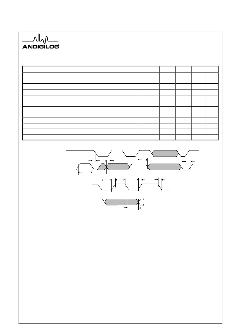
Serial Port Timing
(T
A
= 25 °C, V
DD
= 3.3V unless otherwise noted, Guaranteed by design, not production tested)
Parameter
Symbol
Min
Typ
Max
Units
SCL Operating Frequency
SCL Clock Transition Time
SCL Clock Low Period
f
SCL
t
T:LH
, t
T:HL
t
LOW
t
HIGH
t
BUF
t
SU:DAT
t
HD:DAT
t
SU:STA
t
HD:STA
t
SU:STO
t
POR
t
TIMEOUT
400
300
kHz
ns
μ
s
μ
s
μ
s
ns
ns
ns
ns
ns
ms
ms
1.3
SCL Clock High Period
0.6
50
Bus free time between a Stop and a new Start Condition
1.3
Data in Set-Up to SCL High
Data Out Stable after SCL Low
SCL Low Set-up to SDA Low (Repeated Start Condition)
SCL High Hold after SDA Low (Start Condition)
SDA High after SCL High (Stop Condition)
Time in which aSC7611 must be operational after a power-on reset
SMBus Time-out before device communication interface reset
10
100
300
600
600
600
25
500
35
Notes (cont’d):
5. These specifications are guaranteed only for the test conditions listed.
6. The accuracy of the aSC7611 is guaranteed when using the thermal diode of Intel Pentium 4, 65nm processors or any thermal
diode with a non-ideality of 1.009 and series resistance of 4.52
. When using a 2N3904 type transistor or an CPU with a
different non-ideality the error band will be typically shifted depending on transistor diode or CPU characteristics. See
applications section for details.
7. Accuracy (expressed in °C) = Difference between the aSC7611 reported output temperature and the temperature being
measured. Local temperature accuracy does not include the effects of self-heating. The rise in temperature due to self-heating
is the product of the internal power dissipation of the aSC7611 and the thermal resistance. See (Note 3) for the thermal
resistance to be used in the self-heating calculation.
8. TUE, total unadjusted error, includes ADC gain, offset, linearity and reference errors. TUE is defined as the “actual
V
in
” to
achieve a given code transition minus the “theoretical
V
in
“ for the same code. Therefore, a positive error indicates that the input
voltage is greater than the theoretical input voltage for a given code. If the theoretical input voltage was applied to an aSC7611
that has positive error, the aSC7611’s reading would be less than the theoretical.
9. This specification is provided only to indicate how often temperature and voltage data is updated. The aSC7611 can be read at
any time without regard to conversion state (and will yield last conversion result).
10. Holding the SMBCLK lines low for a time interval greater than t
TIMEOUT
will reset the aSC7611’s SMBus state machine, therefore
setting the SMBDAT pin to a high impedance state.
t
HD:STA
t
SU:STO
t
SU:DAT
SCL
SDA
t
BUF
t
SU:STA
t
HD:DAT
SCL
SDA
Data Out
10
10
90
t
T:LH
t
T:HL
t
LOW
t
HIGH
90
相關(guān)PDF資料 |
PDF描述 |
|---|---|
| ASC7611QS24 | HARDWARE MONITOR WITH INTEGRATED FAN CONTROL |
| ASC7621 | HARDWARE MONITOR WITH INTEGRATED FAN CONTROL |
| ASC7621QS24 | HARDWARE MONITOR WITH INTEGRATED FAN CONTROL |
| ASD05H-12S5 | Isolated and Regulated 5 WATT Open Frame DC/DC Converter |
| ASD05H-12S9 | Isolated and Regulated 5 WATT Open Frame DC/DC Converter |
相關(guān)代理商/技術(shù)參數(shù) |
參數(shù)描述 |
|---|---|
| ASC7611QS24 | 制造商:未知廠家 制造商全稱:未知廠家 功能描述:HARDWARE MONITOR WITH INTEGRATED FAN CONTROL |
| ASC7621 | 制造商:未知廠家 制造商全稱:未知廠家 功能描述:HARDWARE MONITOR WITH INTEGRATED FAN CONTROL |
| ASC7621QS24 | 制造商:未知廠家 制造商全稱:未知廠家 功能描述:HARDWARE MONITOR WITH INTEGRATED FAN CONTROL |
| ASC-8-2-CB (5-PIN) | 制造商:Belden Inc 功能描述:ASC-8-2-CB (5-PIN) |
| ASC-8-2-LED PUR 10M(5-CONTACT) | 制造商:Belden Inc 功能描述:ASC-8-2-LED PUR 10M(5-CONTACT) |
發(fā)布緊急采購,3分鐘左右您將得到回復(fù)。