- 您現(xiàn)在的位置:買賣IC網(wǎng) > PDF目錄369514 > BT16373BDL (NXP SEMICONDUCTORS) 16-bit transparent latch 3-State PDF資料下載
參數(shù)資料
| 型號(hào): | BT16373BDL |
| 廠商: | NXP SEMICONDUCTORS |
| 元件分類: | 通用總線功能 |
| 英文描述: | 16-bit transparent latch 3-State |
| 中文描述: | ABT SERIES, DUAL 8-BIT DRIVER, TRUE OUTPUT, PDSO48 |
| 封裝: | 7.50 MM, PLASTIC, SOT-370-1, SSOP-48 |
| 文件頁(yè)數(shù): | 2/10頁(yè) |
| 文件大小: | 86K |
| 代理商: | BT16373BDL |

Philips Semiconductors
Product specification
74ABT16373B
74ABTH16373B
16-bit transparent latch (3-State)
2
1998 Feb 27
853-1751 19027
FEATURES
16-bit transparent latch
Multiple V
CC
and GND pins minimize switching noise
Power-up 3-State
Live insertion/extraction permitted
Power-up reset
3-State output buffers
74ABTH16373B incorporates bus-hold data inputs which
eliminate the need for external pull-up resistors to hold unused
inputs
Output capability: +64mA/–32mA
I
CCL
–19 mA maximum
Latch-up protection exceeds 500mA per JEDEC Std 17
ESD protection exceeds 2000V per MIL STD 883 Method 3015
and 200V per Machine Model
DESCRIPTION
The 74ABT16373B high-performance BiCMOS device combines
low static and dynamic power dissipation with high speed and high
output drive.
The 74ABT16373B device is a dual octal transparent latch coupled
to two sets of eight 3-State output buffers. The two sections of the
device are controlled independently by Enable (nE) and Output
Enable (nOE) control gates.
The data on each set of D inputs are transferred to the latch outputs
when the Latch Enable (nE) input is High. The latch remains
transparent to the data inputs while nE is High, and stores the data
that is present one setup time before the High-to-Low enable
transition.
The 3-State output buffers are designed to drive heavily loaded
3-State buses, MOS memories, or MOS microprocessors. Each
active-Low Output Enable (nOE) controls eight 3-State buffers
independent of the latch operation.
When nOE is Low, the latched or transparent data appears at the
outputs. When nOE is High, the outputs are in the High-impedance
“OFF” state, which means they will neither drive nor load the bus.
Two options are available, 74ABT16373B which does not have the
bus-hold feature and 74ABTH16373B which incorporates the
bus-hold feature.
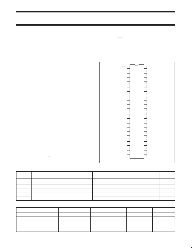
PIN CONFIGURATION
1
2
3
4
5
6
7
8
9
10
11
12
13
14
15
16
17
18
19
20
21
22
23
24
48
47
46
45
44
43
42
41
40
39
38
37
36
35
34
33
32
31
30
29
28
27
26
25
1OE
1Q0
1Q1
GND
1Q2
1Q3
1Q4
1Q5
GND
1Q6
1Q7
2Q0
2Q1
GND
2Q3
V
CC
2Q4
V
CC
2Q2
2Q5
GND
2Q7
2OE
2Q6
1E
1D0
1D1
GND
1D2
1D3
1D4
1D5
GND
1D6
1D7
2D0
2D1
GND
2D3
V
CC
2D4
V
CC
2D2
2D5
GND
2D7
2E
2D6
SA00379
QUICK REFERENCE DATA
SYMBOL
PARAMETER
CONDITIONS
T
amb
= 25
°
C; GND = 0V
TYPICAL
UNIT
t
PLH
t
PHL
C
IN
C
OUT
I
CCZ
I
CCL
Propagation delay
Dn to Qn
Input capacitance
Output capacitance
C
L
= 50pF; V
CC
= 5V
2.5
2.0
4
7
500
8
ns
V
I
= 0V or V
CC
V
O
= 0V or V
CC
; 3-State
Outputs disabled; V
CC
= 5.5V
Outputs low; V
CC
= 5.5V
pF
pF
μ
A
mA
Quiescent supply current
ORDERING INFORMATION
PACKAGES
TEMPERATURE RANGE
OUTSIDE NORTH AMERICA
NORTH AMERICA
DWG NUMBER
48-Pin SSOP type III
–40
°
C to +85
°
C
74ABT16373B DL
BT16373B DL
SOT370-1
48-Pin TSSOP type II
–40
°
C to +85
°
C
74ABT16373B DGG
BT16373B DGG
SOT362-1
48-Pin SSOP type III
–40
°
C to +85
°
C
74ABTH16373B DL
BH16373B DL
SOT370-1
48-Pin TSSOP type II
–40
°
C to +85
°
C
74ABTH16373B DGG
BH16373B DGG
SOT362-1
相關(guān)PDF資料 |
PDF描述 |
|---|---|
| BT16374BDGG | 16-bit D-type flip-flop; positive-edge trigger 3-State |
| BT16374BDL | 16-bit D-type flip-flop; positive-edge trigger 3-State |
| BT16500CDGG | 18-bit universal bus transceiver 3-State |
| BT16500CDL | 18-bit universal bus transceiver 3-State |
| BT16501ADGG | 18-bit universal bus transceiver 3-State |
相關(guān)代理商/技術(shù)參數(shù) |
參數(shù)描述 |
|---|---|
| BT16374BDGG | 制造商:PHILIPS 制造商全稱:NXP Semiconductors 功能描述:16-bit D-type flip-flop; positive-edge trigger 3-State |
| BT16374BDL | 制造商:PHILIPS 制造商全稱:NXP Semiconductors 功能描述:16-bit D-type flip-flop; positive-edge trigger 3-State |
| BT16500CDGG | 制造商:PHILIPS 制造商全稱:NXP Semiconductors 功能描述:18-bit universal bus transceiver 3-State |
| BT16500CDL | 制造商:PHILIPS 制造商全稱:NXP Semiconductors 功能描述:18-bit universal bus transceiver 3-State |
| BT16501ADGG | 制造商:PHILIPS 制造商全稱:NXP Semiconductors 功能描述:18-bit universal bus transceiver 3-State |
發(fā)布緊急采購(gòu),3分鐘左右您將得到回復(fù)。