- 您現(xiàn)在的位置:買賣IC網(wǎng) > PDF目錄166633 > BU3081FV 36.864 MHz, VIDEO CLOCK GENERATOR, PDSO28 PDF資料下載
參數(shù)資料
| 型號: | BU3081FV |
| 元件分類: | 時(shí)鐘產(chǎn)生/分配 |
| 英文描述: | 36.864 MHz, VIDEO CLOCK GENERATOR, PDSO28 |
| 封裝: | SSOP-28 |
| 文件頁數(shù): | 7/8頁 |
| 文件大?。?/td> | 124K |
| 代理商: | BU3081FV |
BU3081FV
Multimedia ICs
Rev.A
7/7
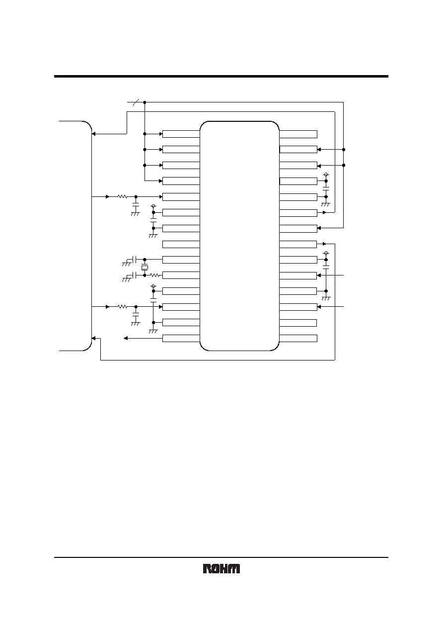
Application circuit
28:VCO_OUT
27:AMCLK_SEL
26:REF_SEL
25:VDD
24:VSS
23:AMCLK_OUT
22:VIDEO_SEL
17:EXT_IN1
18:VSS_EX
16:OE
15:TEST
19:EXT_IN2
21:VCLK_OUT
20:VDD_EX
BU3081FV
27MHz
Control clock supplied
from outside
IEEE1394
Controller
Audio Clock
Audio Loop
PWM
DV Codec
Block
Video Loop
PWM
Video Clock
1:AFS1
2:AFS2
3:FS1
4:FS2
8:SET_R
9:XTAL_IN
10:XTAL_OUT
14:VCXO_OUT
12:VCXO_CTRL
13:VSS_V
11:VDD
5:VCO_CTRL
6:AVDD
7:AVSS
Input for external clock
27MHz 110ppm
+
Note 1) When OE is L, Pin14 : VCXO_OUT, Pin21 : VCLK_OUT, Pin23 : AMCLK_OUT, Pin28 : VCO_OUT become L.
Note 2) Pin8 : SET_R is set to OPEN.
Note 3) When Pin17 : EXT_IN1 is not used, set VIDEO_SEL to OPEN or L, and input the output clock of Pin28 : VCO_OUT
into Pin17.
Note 4) When a crystal is not connected and VCXO is not used, set VIDEO_SEL to H and input the same external clock into
Pin9 : XTAL_IN as Pin17 : EXT_IN1. Set VCXO_CTRL to L, and set VCXO_OUT and XTAL_OUT to OPEN.
Note 5) When neither VCXO nor Pin17 : EXT_IN1 is not used, set EXT_IN1, VCXO_CTRL to L, set VIDEO_SET to OPEN or
L, and set VCXO_OUT, VCLK_OUT, XTAL_IN, and XTAL_OUT to OPEN.
Note 6) When Pin5 : VCO_CTRL is not used, set it to L.
Note 7) When Pin28 : VCO_OUT or Pin23 : AMCLK_OUT is not used, set them to OPEN.
Note 8) When Pin19 : EXT_IN2 is not used, set it to L.
Note 9) Pin15 : TEST is set to OPEN (or L).
Note10) The VCXO operation is checked by using the crystal (specification No. EXS00A-00460) made by NDK (Nihon
Dempa Kogyo Co., LTD). Condition : normal temperature, applied voltage 3.3V
Finally, the crystal needs to be tuned to each set for adjustment f=27MHz at the time of VCXO_CTRL=1.65V
and cancel of temperature characteristic. Please ask a crystal maker.
Note11) BU3081 is basically placed on the board.
Decoupling capacitance (0.1
F) need to be placed between Pin6 (AVDD) and Pin7 (AVSS), Pin11 (VDD_V) and
Pin13 (VSS_V), Pin20 (VDD_EX) and Pin18 (VSS_EX), Pin25 (VDD) and Pin24 (VSS).
To obtain accurate frequency, capacitance (pF) need to be placed between Pin9 and Pin13, Pin10 and Pin13
Tantalum capacitance (10
100pF), ferrite beads may need to be placed to prevent power supply drop in certain
boards case. To reduce high frequency noise, selected bypass capacitors( 1
at problem high frequency)
may be used for power pin as close to BU3081FV as possible.
Note12) ROHM assumes no responsibility for connection of application circuit and use of external components
and component's constant described herein, conveys no license under any patent or other right, and makes
no representation that the circuit are free from patent infringement.
<
相關(guān)PDF資料 |
PDF描述 |
|---|---|
| BU38603 | 8-BIT, MROM, 8 MHz, MICROCONTROLLER, PQFP80 |
| BU38803 | 8-BIT, MROM, 8 MHz, MICROCONTROLLER, PQFP80 |
| BU38905 | 8-BIT, MROM, MICROCONTROLLER, PQFP80 |
| BU4346G | 1-CHANNEL POWER SUPPLY SUPPORT CKT, PDSO5 |
| BU4931FVE-TR | 1-CHANNEL POWER SUPPLY SUPPORT CKT, PDSO5 |
相關(guān)代理商/技術(shù)參數(shù) |
參數(shù)描述 |
|---|---|
| BU3087FV-E | 制造商:ROHM 制造商全稱:Rohm 功能描述:Built in VCXO,Spread-Spectrum Clock Generator |
| BU3087FV-E2 | 制造商:ROHM Semiconductor 功能描述:PLL Clock Generator Single 16-Pin SSOP-B T/R |
| BU-30BL | 功能描述:測試電夾 BRLD MINI-GATOR CLIP RoHS:否 制造商:Pomona Electronics 類型:Minigrabber clip 顏色:Black |
| BU-30C | 功能描述:測試電夾 MIN-GATOR CLIP COP RoHS:否 制造商:Pomona Electronics 類型:Minigrabber clip 顏色:Black |
| BU-30G | 功能描述:CLIP MINI ALLIGATOR 5A GOLD 制造商:mueller electric co 系列:BU 零件狀態(tài):在售 類型:短頭鱷魚夾,迷你型 開度:0.188"(4.79mm)3/16" 電壓 - 額定:- 額定電流:5A 材料:鋼 鍍層:金 材料 - 絕緣:聚氯乙烯(PVC) 絕緣:絕緣 顏色:天然 長度:1.094"(27.79mm) 端接:壓接或焊接 數(shù)量:1 件 等級:- 標(biāo)準(zhǔn)包裝:1 |
發(fā)布緊急采購,3分鐘左右您將得到回復(fù)。