- 您現(xiàn)在的位置:買賣IC網(wǎng) > PDF目錄295171 > BU52021HFV-TR MAGNETIC FIELD SENSOR-HALL EFFECT, 0.8-5.5mT, 0.40-2.60V, RECTANGULAR, SURFACE MOUNT PDF資料下載
參數(shù)資料
| 型號: | BU52021HFV-TR |
| 元件分類: | Magnetic Field Sensor |
| 英文描述: | MAGNETIC FIELD SENSOR-HALL EFFECT, 0.8-5.5mT, 0.40-2.60V, RECTANGULAR, SURFACE MOUNT |
| 封裝: | ROHS COMPLIANT, HVSOF-5 |
| 文件頁數(shù): | 9/21頁 |
| 文件大小: | 866K |
| 代理商: | BU52021HFV-TR |

17/20
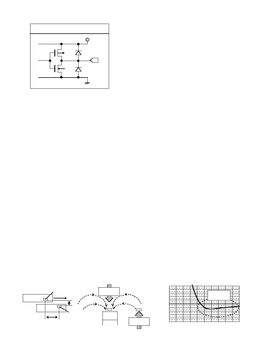
●Terminal Equivalent Circuit Diagram
OUT , OUT1, OUT2
●Operation Notes
1) Absolute maximum ratings
Exceeding the absolute maximum ratings for supply voltage, operating conditions, etc. may result in damage to or
destruction of the IC. Because the source (short mode or open mode) cannot be identified if the device is damaged in this
way, it is important to take physical safety measures such as fusing when implementing any special mode that operates in
excess of absolute rating limits.
2) GND voltage
Make sure that the GND terminal potential is maintained at the minimum in any operating state, and is always kept lower
than the potential of all other pins.
3) Thermal design
Use a thermal design that allows for sufficient margin in light of the power dissipation (Pd) in actual operating conditions.
4) Pin shorts and mounting errors
Use caution when positioning the IC for mounting on printed circuit boards. Mounting errors, such as improper positioning or
orientation, may damage or destroy the device. The IC may also be damaged or destroyed if output pins are shorted
together, or if shorts occur between the output pin and supply pin or GND.
5) Positioning components in proximity to the Hall IC and magnet
Positioning magnetic components in close proximity to the Hall IC or magnet may alter the magnetic field, and therefore the
magnetic detection operation. Thus, placing magnetic components near the Hall IC and magnet should be avoided in the
design if possible. However, where there is no alternative to employing such a design, be sure to thoroughly test and
evaluate performance with the magnetic component(s) in place to verify normal operation before implementing the design.
6) Slide-by position sensing
Fig.42 depicts the slide-by configuration employed for position sensing. Note that when the gap (d) between the magnet and
the Hall IC is narrowed, the reverse magnetic field generated by the magnet can cause the IC to malfunction. As seen in
Fig.43, the magnetic field runs in opposite directions at Point A and Point B. Since the bipolar detection Hall IC can detect
the S-pole at Point A and the N-pole at Point B, it can wind up switching output ON as the magnet slides by in the process of
position detection. Fig. 44 plots magnetic flux density during the magnet slide-by. Although a reverse magnetic field was
generated in the process, the magnetic flux density decreased compared with the center of the magnet. This demonstrates
that slightly widening the gap (d) between the magnet and Hall IC reduces the reverse magnetic field and prevents
malfunctions.
GND
VDD
Fig.41
Because they are configured for CMOS (inverter) output, the
output pins require no external resistance and allow direct
connection to the PC. This, in turn, enables reduction of the
current that would otherwise flow to the external resistor
during magnetic field detection, and supports overall low
current (micropower) operation.
L
d
Magnet
Hall IC
Slide
Fig.42
-10
-8
-6
-4
-2
0
2
4
6
8
10
0
123
456
789
10
Horizontal distance from the magnet [mm]
Magnetic
fux
density[mT]
Reverse
Fig.44
Fig.43
B
S
A
N
Flux
相關PDF資料 |
PDF描述 |
|---|---|
| BU806AU | 8 A, 200 V, NPN, Si, POWER TRANSISTOR |
| BUL43BBS | 2 A, 350 V, NPN, Si, POWER TRANSISTOR |
| BUL43BBU | 2 A, 350 V, NPN, Si, POWER TRANSISTOR |
| BUS-65143-883B | 2 CHANNEL(S), 1M bps, MIL-STD-1553 CONTROLLER, CQIP78 |
| BUS-65145-883B | 2 CHANNEL(S), 1M bps, MIL-STD-1553 CONTROLLER, DFP78 |
相關代理商/技術參數(shù) |
參數(shù)描述 |
|---|---|
| BU52025G | 制造商:ROHM Semiconductor 功能描述:Hole IC,Bop=+/-3.7mT,CMOSout,SSOP5 |
| BU52025G-TR | 功能描述:板機接口霍耳效應/磁性傳感器 2.4-3.6V; +/-3.7mT Bipolar Detection RoHS:否 制造商:Honeywell 類型:Bipolar Hall-Effect Digital Position Sensor 工作電源電壓:3 V to 24 V 電源電流:3.5 mA 最大輸出電流:20 mA 工作點最小值/最大值:5 G, 55 G 最小/最大釋放點(Brp):- 55 G, - 5 G 最大工作溫度:+ 150 C 安裝風格:SMD/SMT 封裝 / 箱體:SOT-23 |
| BU52025G-TR-CUT TAPE | 制造商:ROHM 功能描述:Silicon Monolithic Integrated Circuit, Hall Effet Switch |
| BU52031NVX-TR | 制造商:ROHM Semiconductor 功能描述:IC BU52031 SERIES |
| BU52040HFV | 制造商:ROHM Semiconductor 功能描述:Hole IC,Bop=+/-3.0mT,CMOSout,HVSOF5 |
發(fā)布緊急采購,3分鐘左右您將得到回復。