- 您現(xiàn)在的位置:買賣IC網(wǎng) > PDF目錄366628 > C9822EQ Up to 5A ULDO linear regulator PDF資料下載
參數(shù)資料
| 型號: | C9822EQ |
| 英文描述: | Up to 5A ULDO linear regulator |
| 中文描述: | 單時鐘驅(qū)動器| SSOP封裝| 24針|塑料 |
| 文件頁數(shù): | 2/19頁 |
| 文件大?。?/td> | 123K |
| 代理商: | C9822EQ |
Direct Rambus
III Clock Generator
Cypress Semiconductor Corporation
525 Los Coches St.
Milpitas, CA 95035. Tel: 408-263-6300, Fax: 408-263-6571
http://www.cypress.com
Document#: 38-07093 Rev. **
05/04/2001
Page 2 of 19
APPROVED PRODUCT
C9822
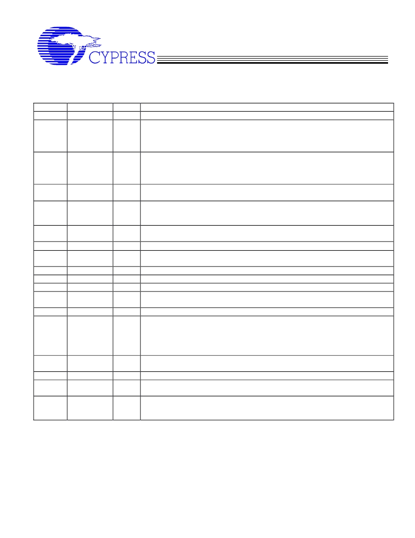
Pin Description
Pin No.
2
6
Pin Name
REFCLK
PCLKM
I/O
I
I
Description
Reference clock input. Normally supplied by a system clock source generator.
Phase detector input: The phase difference between this signal and SYNCLKN is
used to synchronize the Rambus
channel Clock with the system clock. Both the
PCLKM and SYNCLKN are provided by the memory controller. If the gear ratio is
not used, connect this pin to ground.
Phase detector input: The phase difference between this signal and PCLKM is
used to synchronize the Rambus
Channel Clock with the system clock. PCLKM
and SYNCLKN are provided by the memory controller. If the gear ratio is not
used, connect this pin to ground.
Clock Stop. When this input is driven to low state, the differential Rambus
channel clocks are disabled.
Power Down. When this input is driven to a logic low level, the differential
Rambus
channel clocks are disabled and the system clock generator is placed
in a power-down mode.
PLL Multiplier Select: These inputs select the PLL prescaler and feedback
dividers to determine the multiply ratio for the PLL from the input REFLCK.
Differential Rambus
channel clock outputs.
These input pins control the operating mode of the device.
7
SYNCLKN
I
11
STOPB
I
12
PWRDNB
I
15, 14
MULT (0:1)
I
18, 20
24, 23
13
19
1
10
9
CLKB, CLK
S0, S1, S2
O
I
NC
-
No Connect. DO NOT CONNECT ANY VOLTAGE LEVELS TO THIS PIN.
Base voltage reference level for the device’s input reference clock.
Base voltage reference for the PCLKM, SYNCLKN, and STOPB.
Power supply connection for the devices phase aligner circuitry. Connected to
3.3V supply.
Power supply for Analog PLL circuitry. Connected to 3.3V supply.
Power supply clock output buffers. Connected to 3.3V supply. Care should be
taken when routing these power supply connections so as to not have their power
supply current is adequately bypassed (as close to the device as possible) and
their switching noise (surges) does not couple into the other device power
supplies.
Power supply ground return connection for the devices phase aligner circuitry.
Connected to system ground.
Reference supply ground for control input signals.
Power supply ground return connection for Analog PLL circuitry. Should be
connected to system ground potential through a well bypassed path.
System Ground for clock output buffers. Care should be taken when routing these
power return connections so as to not have their power return current shared with
other power return paths of the device.
A bypass capacitor (0.1
μ
F) should be placed as close as possible to each Vdd pin. If these bypass
capacitors are not close to the pins their high frequency filtering characteristic will be canceled by the lead
inductance’s of the traces.
VDDIR
VDDIPD
VDDC
RefV
RefV
P
3
VDDP
VDDO
P
P
16, 22
8
VSSC
P
5
4
VSSI
VSSP
P
P
17, 21
VSSO
P
相關(guān)PDF資料 |
PDF描述 |
|---|---|
| C9827JT | Up to 5A ULDO linear regulator |
| C9827JY | Up to 5A ULDO linear regulator |
| C9832HT | Up to 5A ULDO linear regulator |
| C9832HY | N-CHANNEL 60V - 0.014 Ohm - 60A TO-220/TO220FP STRIPFET POWER MOSFET |
| C9860-21 | 3 BAND EQUALIZER AUDIO PROCESSOR WITH SUBWOOFER CONTROL |
相關(guān)代理商/技術(shù)參數(shù) |
參數(shù)描述 |
|---|---|
| C98-24379-02 | 制造商:CPI 功能描述: |
| C9827H | 制造商:CYPRESS 制造商全稱:Cypress Semiconductor 功能描述:High Performance Pentium 4 Clock Synthesizer |
| C9827HT | 制造商:CYPRESS 制造商全稱:Cypress Semiconductor 功能描述:High Performance Pentium 4 Clock Synthesizer |
| C9827HY | 制造商:CYPRESS 制造商全稱:Cypress Semiconductor 功能描述:High Performance Pentium 4 Clock Synthesizer |
| C9827JT | 制造商:未知廠家 制造商全稱:未知廠家 功能描述:CPU SYSTEM CLOCK GENERATOR|TSSOP|56PIN|PLASTIC |
發(fā)布緊急采購,3分鐘左右您將得到回復(fù)。