- 您現(xiàn)在的位置:買賣IC網(wǎng) > PDF目錄17060 > CDB4382A (Cirrus Logic Inc)BOARD EVAL FOR CS4382A DAC PDF資料下載
參數(shù)資料
| 型號: | CDB4382A |
| 廠商: | Cirrus Logic Inc |
| 文件頁數(shù): | 24/50頁 |
| 文件大?。?/td> | 0K |
| 描述: | BOARD EVAL FOR CS4382A DAC |
| 標(biāo)準(zhǔn)包裝: | 1 |
| DAC 的數(shù)量: | 8 |
| 位數(shù): | 24 |
| 采樣率(每秒): | 192k |
| 數(shù)據(jù)接口: | 串行 |
| DAC 型: | 電壓 |
| 工作溫度: | -40°C ~ 85°C |
| 已供物品: | 板 |
| 已用 IC / 零件: | CS4382A |
| 產(chǎn)品目錄頁面: | 757 (CN2011-ZH PDF) |
| 相關(guān)產(chǎn)品: | CS4382A-DQZR-ND - IC DAC 8CH 114DB 192KHZ 48-LQFP CS4382A-DQZ-ND - IC DAC 8CH 114DB 192KHZ 48-LQFP CS4382A-CQZR-ND - IC DAC 8CH 114DB 192KHZ 48-LQFP 598-1061-ND - IC DAC 8CH 114DB 192KHZ 48LQFP |
| 其它名稱: | 598-1524 |
第1頁第2頁第3頁第4頁第5頁第6頁第7頁第8頁第9頁第10頁第11頁第12頁第13頁第14頁第15頁第16頁第17頁第18頁第19頁第20頁第21頁第22頁第23頁當(dāng)前第24頁第25頁第26頁第27頁第28頁第29頁第30頁第31頁第32頁第33頁第34頁第35頁第36頁第37頁第38頁第39頁第40頁第41頁第42頁第43頁第44頁第45頁第46頁第47頁第48頁第49頁第50頁
30
DS618F2
CS4382A
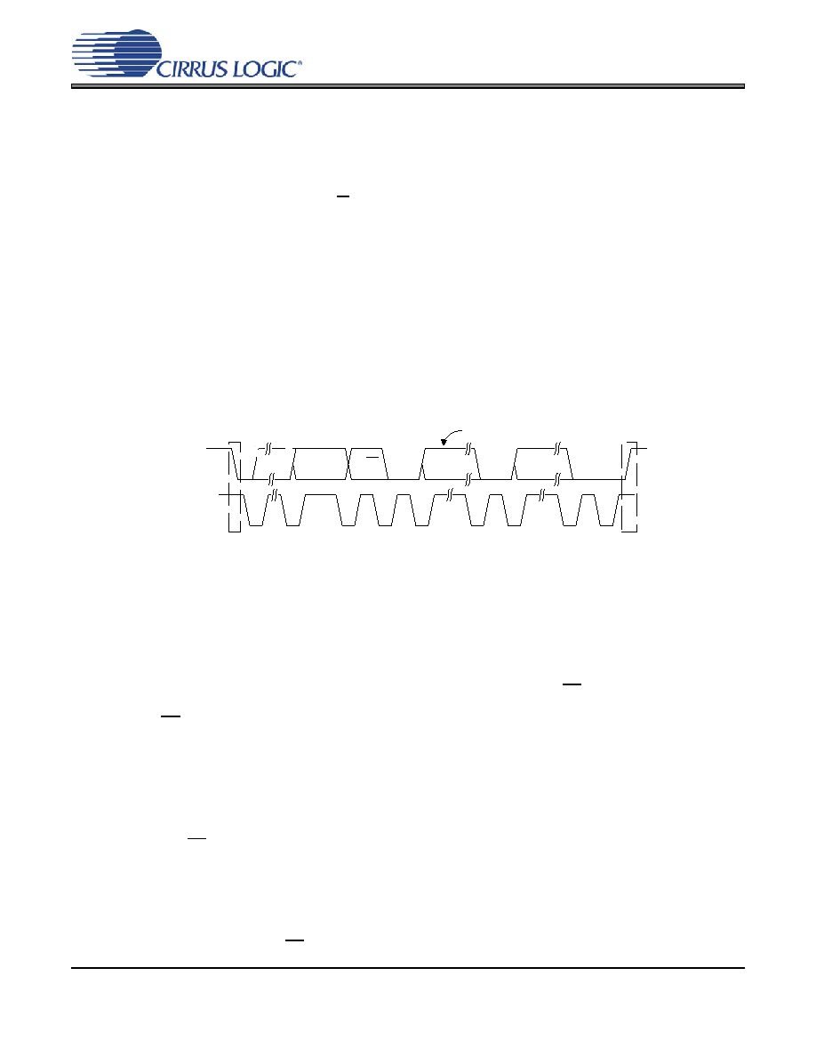
4.14.2.2 IC Read
To read from the device, follow the procedure below while adhering to the Control Port Switching Speci-
fications.
1. Initiate a START condition to the IC bus followed by the address byte. The upper 6 bits must be
001100. The seventh bit must match the setting of the AD0 pin, and the eighth must be 1. The eighth
bit of the address byte is the R/W bit.
2. After transmitting an acknowledge (ACK), the device will then transmit the contents of the register
pointed to by the MAP. The MAP register will contain the address of the last register written to the
MAP, or the default address (see Section 4.14.1) if an IC read is the first operation performed on the
device.
3. Once the device has transmitted the contents of the register pointed to by the MAP, issue an ACK.
4. If the INCR bit is set to 1, the device will continue to transmit the contents of successive registers. Con-
tinue providing a clock and issue an ACK after each byte until all the desired registers are read; then
initiate a STOP condition to the bus.
5. If the INCR bit is set to 0 and further IC reads from other registers are desired, it is necessary to initiate
a repeated START condition and follow the procedure detailed from steps 1 and 2 from the IC Write
instructions followed by step 1 of the IC Read section. If no further reads from other registers are de-
sired, initiate a STOP condition to the bus.
4.14.3
SPI Mode
In SPI Mode, data is clocked into the serial control data line, CDIN, by the serial Control Port clock, CCLK
(see Figure 19 for the clock-to-data relationship). There is no AD0 pin. Pin CS is the chip select signal and
is used to control SPI writes to the Control Port. When the device detects a high-to-low transition on the
AD0/CS pin after power-up, SPI Mode will be selected. All signals are inputs and data is clocked in on the
rising edge of CCLK.
4.14.3.1 SPI Write
To write to the device, follow the procedure below while adhering to the Control Port Switching Specifica-
tions in Section 2.
1. Bring CS low.
2. The address byte on the CDIN pin must then be 00110000.
3. Write to the memory address pointer, MAP. This byte points to the register to be written.
4. Write the desired data to the register pointed to by the MAP.
5. If the INCR bit (see Section 4.14.1) is set to 1, repeat the previous step until all the desired registers
are written, then bring CS high.
SD A
SC L
0011 00
ADD R
AD 0
R/W
Sta rt
ACK
DAT A
1-8
AC K
DA T A
1-8
ACK
Stop
N o te : If o pe ra tion is a w rite , th is b y te c on ta in s the M e m o ry A ddre s s P o inter, M A P .
No te 1
Figure 18. Control Port Timing, IC Mode
相關(guān)PDF資料 |
PDF描述 |
|---|---|
| 0210490183 | CABLE JUMPER 1.25MM .229M 12POS |
| VE-B3V-EY | CONVERTER MOD DC/DC 5.8V 50W |
| UPTW6181MRD | CAP ALUM 180UF 420V 20% RADIAL |
| CDB4362A | BOARD EVAL FOR CS4362A DAC |
| YLCDRSK1668S | KIT DEMONSTRATION LCD H8SX1668 |
相關(guān)代理商/技術(shù)參數(shù) |
參數(shù)描述 |
|---|---|
| CDB4383 | 制造商:CIRRUS 制造商全稱:Cirrus Logic 功能描述:114 dB, 192 kHz 8-Channel D/A Converter |
| CDB4384 | 功能描述:音頻 IC 開發(fā)工具 Eval Bd 8-Ch DAC w/DSD RoHS:否 制造商:Texas Instruments 產(chǎn)品:Evaluation Kits 類型:Audio Amplifiers 工具用于評估:TAS5614L 工作電源電壓:12 V to 38 V |
| CDB4385 | 功能描述:音頻 IC 開發(fā)工具 Eval Bd 8-Ch DAC w/DSD RoHS:否 制造商:Texas Instruments 產(chǎn)品:Evaluation Kits 類型:Audio Amplifiers 工具用于評估:TAS5614L 工作電源電壓:12 V to 38 V |
| CDB4390 | 制造商:CIRRUS 制造商全稱:Cirrus Logic 功能描述:24-Bit, Stereo D/A Converter for Digital Audio |
| CDB4391 | 制造商:CIRRUS 制造商全稱:Cirrus Logic 功能描述:24-Bit, 192 kHz Stereo DAC with Volume Control |
發(fā)布緊急采購,3分鐘左右您將得到回復(fù)。