- 您現(xiàn)在的位置:買賣IC網(wǎng) > PDF目錄298968 > CS3865CGDWR16 (ON SEMICONDUCTOR) 1 A DUAL SWITCHING CONTROLLER, 500 kHz SWITCHING FREQ-MAX, PDSO16 PDF資料下載
參數(shù)資料
| 型號: | CS3865CGDWR16 |
| 廠商: | ON SEMICONDUCTOR |
| 元件分類: | 穩(wěn)壓器 |
| 英文描述: | 1 A DUAL SWITCHING CONTROLLER, 500 kHz SWITCHING FREQ-MAX, PDSO16 |
| 封裝: | 0.300 INCH, MS-013, SO-16 |
| 文件頁數(shù): | 2/8頁 |
| 文件大?。?/td> | 82K |
| 代理商: | CS3865CGDWR16 |
2
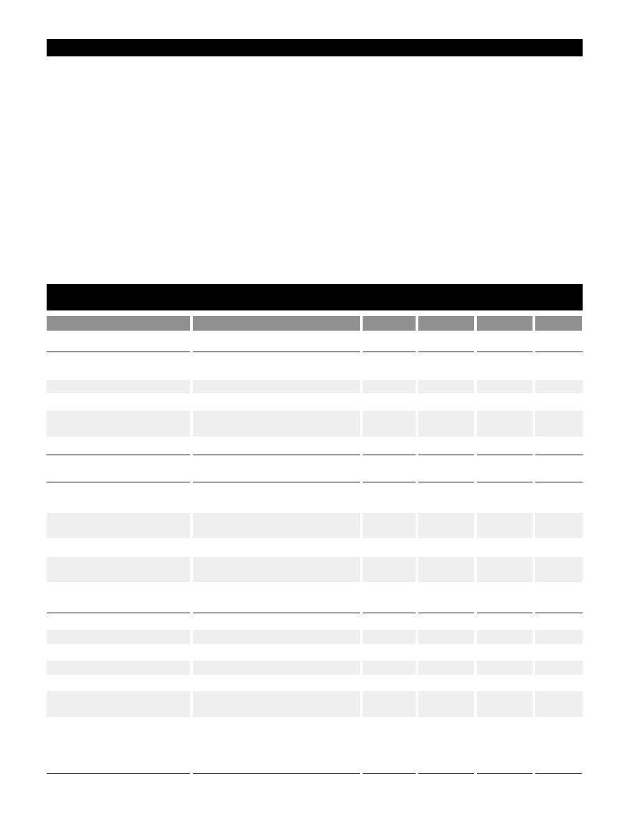
Electrical Characteristics: VCC = 15V, RT = 8.2k, CT = 3.3nF, for typical values TA=25°C, for min/max values TA is the operating
ambient temperature range that applies [Note 3].
PARAMETER
TEST CONDITIONS
MIN
TYP
MAX
UNIT
Absolute Maximum Ratings
Total Power Supply and Zener Current .........................................................................................................................50mA
Output Current, Source or Sink (Note 1)...........................................................................................................................1.0A
Output Energy (capacitive load per cycle) .......................................................................................................................5.0J
Current Sense, Enable and Voltage ......................................................................................................................-0.3 to +5.5V
Feedback Inputs
High State (Voltage)..........................................................................................................................................5.5V
Low State (Reverse Current) ......................................................................................................................-5.0mA
Error Amp Output Sink Current......................................................................................................................................10mA
Storage Temperature Range ................................................................................................................................-65 to +150°C
Operating Junction Temperature...................................................................................................................................+150°C
Operating Ambient Temperature.............................................................................................................................0 to +70°C
Lead Temperature Soldering
Wave Solder (through hole styles only) .................................................................................10 sec. max, 260°C peak
Reflow (SMD styles only) ..................................................................................60 sec. max above 183°C, 230°C peak
CS3865C
s Reference Section
Reference Output Voltage,
IOUT=1.0mA, TJ=25°C
4.9
5.0
5.1
V
VREF
Line Regulation
11V
≤V
CC≤15V
2.0
20.0
mV
Load Regulation
1.0mA
≤I
OUT≤10mA
3.0
25.0
mV
Total Output Variation over
4.85
5.15
V
Line, Load and Temperature
Output Short Circuit Current
30
100
mA
s Oscillator and PWM Sections
Total Frequency Variation
11V
≤V
CC≤15V, Tlow≤TA≤Thigh
46.5
49.0
51.5
kHz
over Line and Temperature
Frequency Change with
11V
≤V
CC≤15V
0.2
1.0
%
Voltage
Duty Cycle at each Output
Maximum
46.0
49.5
52.0
%
Sync Input Current
High State VIN=2.4V
170
250
A
Low State VIN=0.8V
80
160
s Error Amplifiers
Voltage Feedback Input
VOUT=2.5V
2.42
2.50
2.58
V
Input Bias Current
VFB=5.0V
-0.1
-1.0
A
Open-Loop Voltage Gain
VOUT=2.0 to 4.0V
65
100
dB
Unity Gain Bandwidth
TJ=25°C (note 6)
0.7
1.0
MHz
Power Supply Rejection Ratio VCC=11V to 15V
60
90
dB
Output Current
Source VOUT=3.0V, VFB=2.3V
-0.45
-1.00
mA
Sink VOUT=1.2V, VFB=2.7V
2.00
12.00
mA
Output Voltage Swing
High State, RL=15k to ground,
VFB=2.3V
5.0
6.2
V
Low State, RL=15k to VREF,
VFB = 2.7V
0.8
1.1
相關(guān)PDF資料 |
PDF描述 |
|---|---|
| CS4112-CS | 1M X 8 MASK PROM, 120 ns, PDSO32 |
| CS4AVH-156M250-4 | CRYSTAL OSCILLATOR, CLOCK, 156.25 MHz, HCMOS OUTPUT |
| CS5101A-TE8 | Single-Ended Data Acquisition System |
| CS5101-BD16 | Single-Ended Data Acquisition System |
| CS5101-BD8 | Single-Ended Data Acquisition System |
相關(guān)代理商/技術(shù)參數(shù) |
參數(shù)描述 |
|---|---|
| CS3865CGN16 | 制造商:CHERRY 制造商全稱:CHERRY 功能描述:High Performance Dual Channel Current Mode Controller with ENABLE |
| CS-3865CN16 | 制造商:未知廠家 制造商全稱:未知廠家 功能描述:Current-Mode SMPS Controller |
| CS386H | 制造商:CHERRY 制造商全稱:CHERRY 功能描述:Alternator Voltage Regulator Darlington Driver |
| CS387 | 制造商:ONSEMI 制造商全稱:ON Semiconductor 功能描述:Alternator Voltage Regulator Darlington Driver |
| CS-387 | 制造商:未知廠家 制造商全稱:未知廠家 功能描述:Automotive Voltage Regulator |
發(fā)布緊急采購,3分鐘左右您將得到回復(fù)。