- 您現(xiàn)在的位置:買賣IC網(wǎng) > PDF目錄298968 > CS3865CGDWR16 (ON SEMICONDUCTOR) 1 A DUAL SWITCHING CONTROLLER, 500 kHz SWITCHING FREQ-MAX, PDSO16 PDF資料下載
參數(shù)資料
| 型號: | CS3865CGDWR16 |
| 廠商: | ON SEMICONDUCTOR |
| 元件分類: | 穩(wěn)壓器 |
| 英文描述: | 1 A DUAL SWITCHING CONTROLLER, 500 kHz SWITCHING FREQ-MAX, PDSO16 |
| 封裝: | 0.300 INCH, MS-013, SO-16 |
| 文件頁數(shù): | 5/8頁 |
| 文件大?。?/td> | 82K |
| 代理商: | CS3865CGDWR16 |

5
The CS3865C is a high performance, fixed frequency, dual
channel current mode PWM controller specifically
designed for off-line and DC to DC converter applications.
It offers the designer a cost effective solution with minimal
external components where independent regulation of two
power converters is required. Each channel contains a high
gain error amplifier, current sensing comparator, pulse
width modulator latch, and totem pole output driver. The
oscillator, reference, and undervoltage lockout circuits are
common to both channels.
The oscillator uses precise frequency and duty cycle con-
trol. The frequency is programmed by the values RT and
CT. Capacitor, CT, is charged and discharged by an equal
magnitude internal current source and sink, generating a
symmetrical 50 percent duty cycle waveform at CT. The
oscillator peak and valley thresholds are 3.5V and 1.6V
respectively. The source/sink current magnitude is con-
trolled by resistor RT. For proper operation over tempera-
ture range, its value should be between 4.0k
and 16k.
As CT charges and discharges, an internal blanking pulse
is generated that alternately drives the inputs of the upper
and lower NOR gates high. This, in conjunction with a
precise amount of delay time introduced into each chan-
nel, produces well defined non-overlapping output duty
cycles. The second output, VOUT
2 is enabled while CT is
charging, and the primary is enabled during the discharge.
Even at 500kHz, each output is capable of approximately
44% duty cycle, making this controller suitable for high
frequency power conversion applications.
In many noise sensitive applications, it may be necessary
to synchronize the converter with an external system
clock. This can be accomplished by applying an external
clock signal. For reliable synchronization, the oscillator fre-
quency should be set about 10% slower than the clock fre-
quency. The rising edge of the clock signal applied to
SYNC, terminates CT‘s charging and VOUT
2‘s conduction.
By tailoring the clock waveform symmetry, accurate duty
cycle clamping of either output can be achieved.
Each channel contains a fully-compensated error amplifi-
er. The output and inverting input nodes are accessible.
The amplifier features a typical dc voltage gain of 100 dB,
and a unity gain bandwidth of 1.0 MHz with 71 degrees of
phase margin. The non-inverting input is internally biased
at 2.5V. The converter output voltage is typically divided
down and monitored by the inverting input through a
resistor divider. The maximum input bias current is -1.0A
which will cause an output voltage error that is equal to
the product of the input bias current and the equivalent
input divider resistance.
Error Amplifier
Oscillator
Operating Description
CS3865C
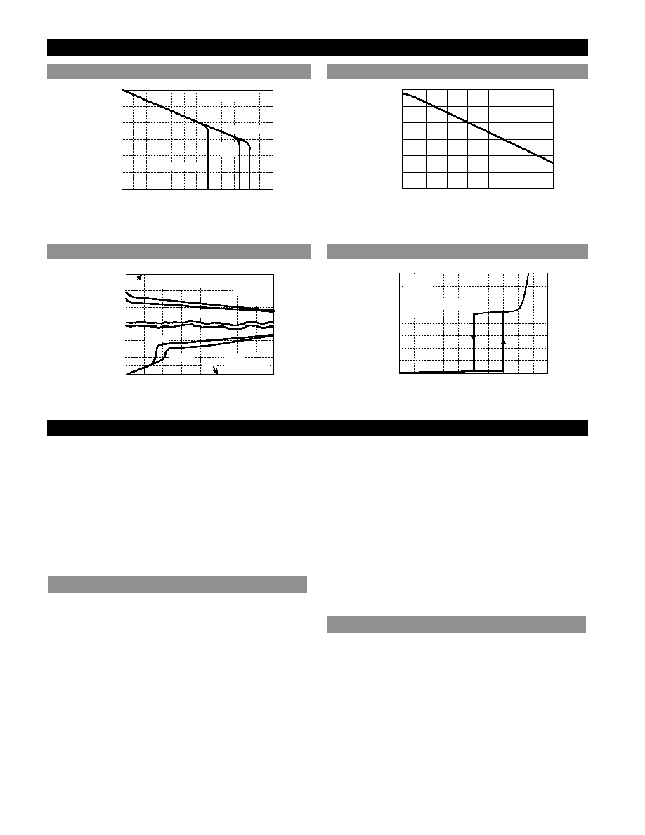
Typical Performance Characteristics: continued
0
20
40
60
80
100
120
I ref, REFERENCE SOURCE CURRENT (mA)
-24
-20
-16
-12
-8.0
-4.0
0
V
REF
,REFERENCE
V
o
ltage
(mV)
VCC = 15V
TA = –55°C
TA = 125°C
TA =
25
°C
-55
-25
0
25
50
75
100
125
TA, AMBIENT TEMPERATURE (°C)
I SC
,REFERENCE
SHOR
T
CIRCUIT
CURRENT
(mA)
120
100
80
60
Reference Short Circuit Current vs. Temperature
Reference Voltage Change vs. Source Current
SOURCE SATURATION
(LOAD TO GROUND)
VCC=15V
80
S PULSED LOAD
120Hz RATE
TA=25°C
TA= –55°C
TA=25°C
SINK
SATURATION
(LOAD TO VCC)
GND
0
200
400
600
800
OUTPUT LOAD CURRENT (mA)
V
sat
,OUTPUT
SA
TURA
TION
VOL
T
AGE
(V)
VCC
0
-1.0
-2.0
2.0
1.0
0
4.0
8.0
12
16
20
VCC, SUPPLY VOLTAGE (V)
0
8.0
16
24
32
RT=8.2k
CT=3.3nF
VFB 1.2=0V
CURRENT SENSE 1.2=0V
TA=25°C
I CC,
SUPPL
Y
CURRENT
(mA)
Supply Current vs. Supply Voltage CS3865C
Output Saturation Voltage vs. Load Current
相關(guān)PDF資料 |
PDF描述 |
|---|---|
| CS4112-CS | 1M X 8 MASK PROM, 120 ns, PDSO32 |
| CS4AVH-156M250-4 | CRYSTAL OSCILLATOR, CLOCK, 156.25 MHz, HCMOS OUTPUT |
| CS5101A-TE8 | Single-Ended Data Acquisition System |
| CS5101-BD16 | Single-Ended Data Acquisition System |
| CS5101-BD8 | Single-Ended Data Acquisition System |
相關(guān)代理商/技術(shù)參數(shù) |
參數(shù)描述 |
|---|---|
| CS3865CGN16 | 制造商:CHERRY 制造商全稱:CHERRY 功能描述:High Performance Dual Channel Current Mode Controller with ENABLE |
| CS-3865CN16 | 制造商:未知廠家 制造商全稱:未知廠家 功能描述:Current-Mode SMPS Controller |
| CS386H | 制造商:CHERRY 制造商全稱:CHERRY 功能描述:Alternator Voltage Regulator Darlington Driver |
| CS387 | 制造商:ONSEMI 制造商全稱:ON Semiconductor 功能描述:Alternator Voltage Regulator Darlington Driver |
| CS-387 | 制造商:未知廠家 制造商全稱:未知廠家 功能描述:Automotive Voltage Regulator |
發(fā)布緊急采購,3分鐘左右您將得到回復(fù)。