- 您現(xiàn)在的位置:買賣IC網(wǎng) > PDF目錄374166 > CS5127GDW16 (ZF Electronics Corporation) Dual Output Nonsynchronous Buck Controller with Sync Function and Second Channel Enable PDF資料下載
參數(shù)資料
| 型號: | CS5127GDW16 |
| 廠商: | ZF Electronics Corporation |
| 英文描述: | Dual Output Nonsynchronous Buck Controller with Sync Function and Second Channel Enable |
| 中文描述: | 非同步雙輸出同步降壓控制器的功能及第二通道啟用 |
| 文件頁數(shù): | 5/24頁 |
| 文件大小: | 293K |
| 代理商: | CS5127GDW16 |
C
5
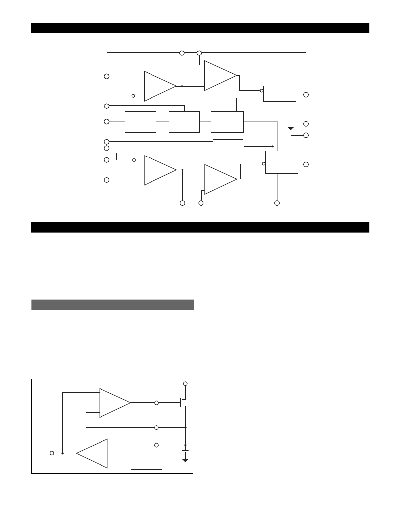
Theory of Operation
The CS5127 is a dual power supply controller that utilizes
the V
2
acontrol method. Two nonsynchronous V
2
abuck
regulators can be built using a single controller IC. This IC
is a perfect choice for efficiently and economically provid-
ing core power and I/O power for the latest
high-performance CPUs. Both switching regulators
employ a fixed frequency architecture driven from a
common oscillator circuit.
The V
2
amethod of control uses a ramp signal generated
by the ESR of the output capacitors. This ramp is propor-
tional to the AC current in the inductor and is offset by the
DC output voltage. V
2
ainherently compensates for varia-
tion in both line and load conditions since the ramp signal
is generated from the output voltage. This differs from tra-
ditional methods such as voltage mode control, where an
artificial ramp signal must be generated, and current mode
control, where a ramp is generated from inductor current.
Figure 1: V
2
acontrol diagram.
The V
2
acontrol method is illustrated in Figure 1. Both
the ramp signal and the error signal are generated by the
output voltage. Since the ramp voltage is defined as the
output voltage, the ramp signal is affected by any change
in the output, regardless of the origin of that change. The
ramp signal also contains the DC portion of the output
voltage, allowing the control circuit to drive the output
switch from 0% to about 90% duty cycle.
Changes in line voltage will change the current ramp in
the inductor, affecting the ramp signal and causing the
V
2
acontrol loop to adjust the duty cycle. Since a change
in inductor current changes the ramp signal, the V
2
a
method has the characteristics and advantages of current
mode control for line transient response.
Changes in load current will affect the output voltage and
thus will also change the ramp signal. A load step will
immediately change the state of the comparator output
that controls the output switch. In this case, load transient
response time is limited by the comparator response time
and the transition speed of the switch. Notice that the reac-
tion time of the V
2
aloop to a load transient is not
dependent on the crossover frequency of the error signal
loop. Traditional voltage mode and current mode methods
are dependent on the compensation of the error signal
loop.
The V
2
aerror signal loop can have a low crossover fre-
quency, since transient response is handled by the ramp
signal loop. The òslowó error signal loop provides DC
accuracy. Low frequency roll-off of the error amplifier
bandwidth will significantly improve noise immunity.
This also improves remote sensing of the output voltage,
since switching noise picked up in long feedback traces
can be effectively filtered.
V
2
aline and load regulation are dramatically improved
because there are two separate control loops. A voltage
COMP
V
FB
GATE
V
FFB
PWM
Comparator
-
+
Reference
Voltage
Error
Amplifier
+
-
Error Signal
Ramp Signal
V
2
aControl Method
Block Diagram
C
T
SYNC
COMP2
COMP1
ENABLE
LGND
V
FB2
V
REF
V
IN
GATE1
GATE2
V
FFB1
V
FFB2
R
T
PGND
Error
Amplifier
-
+
1.275V
PWM
Comparator
+
-
Channel 2
Gate Driver
Oscillator
Reference
Undervoltage
Lockout
Bandgap
Voltage
Reference
V
Undervoltage
Lockout
Channel 2
Gate Driver
Error
Amplifier
+
-
1.275V
V
FB1
PWM
Comparator
-
+
相關PDF資料 |
PDF描述 |
|---|---|
| CS5127GDWR16 | Dual Output Nonsynchronous Buck Controller with Sync Function and Second Channel Enable |
| CS5127 | Dual Output Nonsynchronous Buck Controller with Sync Function and Second Channel Enable |
| CS51311GDR14 | Synchronous CPU Buck Controller for 12V and 5V Applications |
| CS51311 | Synchronous CPU Buck Controller for 12V and 5V Applications |
| CS51311GD14 | Synchronous CPU Buck Controller for 12V and 5V Applications |
相關代理商/技術參數(shù) |
參數(shù)描述 |
|---|---|
| CS5127GDWR16 | 制造商:Rochester Electronics LLC 功能描述:- Bulk |
| CS5128AF | 制造商:Rochester Electronics LLC 功能描述:- Bulk |
| CS5-12IO2 | 制造商:未知廠家 制造商全稱:未知廠家 功能描述:Netzthyristoren Phase control thyristors |
| CS51311GD14 | 制造商:Rochester Electronics LLC 功能描述:- Bulk |
| CS-51313D16 | 制造商:未知廠家 制造商全稱:未知廠家 功能描述:Current-Mode SMPS Controller |
發(fā)布緊急采購,3分鐘左右您將得到回復。