- 您現(xiàn)在的位置:買賣IC網(wǎng) > PDF目錄170342 > CXK77P18L80AGB-4A 512K X 18 LATE-WRITE SRAM, 3.8 ns, PBGA119 PDF資料下載
參數(shù)資料
| 型號: | CXK77P18L80AGB-4A |
| 元件分類: | SRAM |
| 英文描述: | 512K X 18 LATE-WRITE SRAM, 3.8 ns, PBGA119 |
| 封裝: | 14 X 22 MM, 1.27 MM PITCH, PLASTIC, BGA-119 |
| 文件頁數(shù): | 20/25頁 |
| 文件大?。?/td> | 269K |
| 代理商: | CXK77P18L80AGB-4A |
SONY
CXK77P36L80AGB / CXK77P18L80AGB
Preliminary
8Mb LW R-L, rev 1.1
4 / 25
May 22, 2002
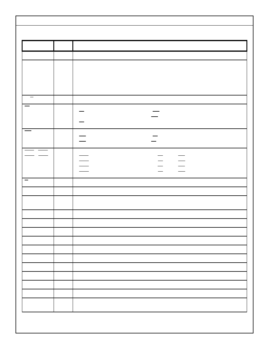
Pin Description
Symbol
Type
Description
SA
Input
Synchronous Address Inputs - Registered on the rising edge of K.
DQa, DQb
DQc, DQd
I/O
Synchronous Data Inputs / Outputs - Registered on the rising edge of K during write operations.
Driven from the falling edge of K during read operations.
DQa - indicates Data Byte a
DQb - indicates Data Byte b
DQc - indicates Data Byte c
DQd - indicates Data Byte d
K, K
Input
Differential Input Clocks
SS
Input
Synchronous Select Input - Registered on the rising edge of K.
SS = 0
specifies a write operation when SW = 0
specifies a read operation when SW = 1
SS = 1
specifies a deselect operation
SW
Input
Synchronous Global Write Enable Input - Registered on the rising edge of K.
SW = 0 specifies a write operation when SS = 0
SW = 1 specifies a read operation when SS = 0
SBWa, SBWb,
SBWc, SBWd
Input
Synchronous Byte Write Enable Inputs - Registered on the rising edge of K.
SBWa = 0 specifies write Data Byte a when SS = 0 and SW = 0
SBWb = 0 specifies write Data Byte b when SS = 0 and SW = 0
SBWc = 0 specifies write Data Byte c when SS = 0 and SW = 0
SBWd = 0 specifies write Data Byte d when SS = 0 and SW = 0
G
Input
Asynchronous Output Enable Input - De-asserted (high) forces the data output drivers to Hi-Z.
ZZ
Input
Asynchronous Sleep Mode Input - Asserted (high) forces the SRAM into low-power mode.
M1, M2
Input
Read Operation Protocol Select - These mode pins must be tied “high” and “l(fā)ow” respectively to
select Register - Latch read operations.
ZQ
Input
Output Impedance Control Resistor Input
VDD
3.3V Core Power Supply - Core supply voltage.
VDDQ
Output Power Supply - Output buffer supply voltage.
VREF
Input Reference Voltage - Input buffer threshold voltage.
VSS
Ground
TCK
Input
JTAG Clock
TMS
Input
JTAG Mode Select
TDI
Input
JTAG Data In
TDO
Output
JTAG Data Out
RSVD
Reserved - This pin is used for Sony test purposes only. It must be left unconnected.
NC
No Connect - These pins are true no-connects, i.e. there is no internal chip connection to these
pins. They can be left unconnected or tied directly to VDD, VDDQ, or VSS.
相關(guān)PDF資料 |
PDF描述 |
|---|---|
| CXO-199-148.5MHZ | CRYSTAL OSCILLATOR, SINE OUTPUT, 148.5 MHz |
| CXO63HT-7I-FREQ1-OUT23 | CRYSTAL OSCILLATOR, CLOCK, 16 MHz - 50 MHz, CMOS/TTL OUTPUT |
| CXO63HT-7I-FREQ2-OUT23 | CRYSTAL OSCILLATOR, CLOCK, 50 MHz - 70 MHz, CMOS/TTL OUTPUT |
| CXO63HT-5C-FREQ3-OUT23 | CRYSTAL OSCILLATOR, CLOCK, 70 MHz - 105.561 MHz, CMOS/TTL OUTPUT |
| CXO65HT-5C-FREQ2-OUT23 | CRYSTAL OSCILLATOR, CLOCK, 50 MHz - 70 MHz, CMOS/TTL OUTPUT |
相關(guān)代理商/技術(shù)參數(shù) |
參數(shù)描述 |
|---|---|
| CXK77P18R160GB | 制造商:未知廠家 制造商全稱:未知廠家 功能描述:MEMORY-UHS Synch SRAMs</A></I> 16Meg Ultra-High-Speed Synchronous SRAM (1M x 18) (22 pages 233K Rev. 6/3/02) |
| CXK77P36E160GB | 制造商:SONY 制造商全稱:Sony Corporation 功能描述:16Mb LW R-L HSTL High Speed Synchronous SRAMs (512K x 36 or 1M x 18) |
| CXK77P36E160GB-42AE | 制造商:SONY 制造商全稱:Sony Corporation 功能描述:16Mb LW R-L HSTL High Speed Synchronous SRAMs (512K x 36 or 1M x 18) |
| CXK77P36E160GB-42BE | 制造商:SONY 制造商全稱:Sony Corporation 功能描述:16Mb LW R-L HSTL High Speed Synchronous SRAMs (512K x 36 or 1M x 18) |
| CXK77P36E160GB-42E | 制造商:SONY 制造商全稱:Sony Corporation 功能描述:16Mb LW R-L HSTL High Speed Synchronous SRAMs (512K x 36 or 1M x 18) |
發(fā)布緊急采購,3分鐘左右您將得到回復(fù)。