- 您現(xiàn)在的位置:買(mǎi)賣(mài)IC網(wǎng) > PDF目錄378502 > CY7C1381C-100AI (CYPRESS SEMICONDUCTOR CORP) 18-Mb (512K x 36/1M x 18) Flow-Through SRAM PDF資料下載
參數(shù)資料
| 型號(hào): | CY7C1381C-100AI |
| 廠商: | CYPRESS SEMICONDUCTOR CORP |
| 元件分類(lèi): | DRAM |
| 英文描述: | 18-Mb (512K x 36/1M x 18) Flow-Through SRAM |
| 中文描述: | 512K X 36 STANDARD SRAM, 8.5 ns, PQFP100 |
| 封裝: | 14 X 20 MM, 1.40 MM HEIGHT, PLASTIC, TQFP-100 |
| 文件頁(yè)數(shù): | 14/36頁(yè) |
| 文件大小: | 564K |
| 代理商: | CY7C1381C-100AI |
第1頁(yè)第2頁(yè)第3頁(yè)第4頁(yè)第5頁(yè)第6頁(yè)第7頁(yè)第8頁(yè)第9頁(yè)第10頁(yè)第11頁(yè)第12頁(yè)第13頁(yè)當(dāng)前第14頁(yè)第15頁(yè)第16頁(yè)第17頁(yè)第18頁(yè)第19頁(yè)第20頁(yè)第21頁(yè)第22頁(yè)第23頁(yè)第24頁(yè)第25頁(yè)第26頁(yè)第27頁(yè)第28頁(yè)第29頁(yè)第30頁(yè)第31頁(yè)第32頁(yè)第33頁(yè)第34頁(yè)第35頁(yè)第36頁(yè)
CY7C1381C
CY7C1383C
Document #: 38-05238 Rev. *B
Page 14 of 36
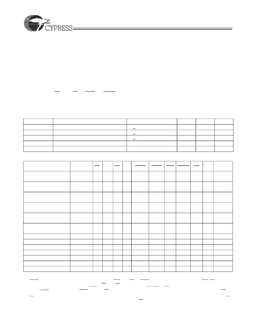
Sleep Mode
The ZZ input pin is an asynchronous input. Asserting ZZ
places the SRAM in a power conservation “sleep” mode. Two
clock cycles are required to enter into or exit from this “sleep”
mode. While in this mode, data integrity is guaranteed.
Accesses pending when entering the “sleep” mode are not
considered valid nor is the completion of the operation
guaranteed. The device must be deselected prior to entering
the “sleep” mode. CE
, CE
, CE
3[2]
, ADSP, and ADSC must
remain inactive for the duration of t
ZZREC
after the ZZ input
returns LOW.
.
ZZ Mode Electrical Characteristics
Parameter
I
DDZZ
t
ZZS
t
ZZREC
t
ZZI
t
RZZI
Truth Table
[ 3, 4, 5, 6, 7]
Description
Test Conditions
ZZ > V
DD
– 0.2V
ZZ > V
DD
– 0.2V
ZZ < 0.2V
This parameter is sampled
This parameter is sampled
Min.
Max.
60
2t
CYC
Unit
mA
ns
ns
ns
ns
Snooze mode standby current
Device operation to ZZ
ZZ recovery time
ZZ active to snooze current
ZZ Inactive to exit snooze current
2t
CYC
2t
CYC
0
Cycle Description
ADDRESS
Used
CE
1
H
CE
2
CE
3
X
ZZ
ADSP
ADSC
ADV WRITE
OE
CLK
DQ
Deselected Cycle,
Power-down
None
X
L
X
L
X
X
X
L-H Tri-State
Deselected Cycle,
Power-down
None
L
L
X
L
L
X
X
X
X
L-H Tri-State
Deselected Cycle,
Power-down
None
L
X
H
L
L
X
X
X
X
L-H Tri-State
Deselected Cycle,
Power-down
None
L
L
X
L
H
L
X
X
X
L-H Tri-State
Deselected Cycle,
Power-down
None
X
X
X
L
H
L
X
X
X
L-H Tri-State
Snooze Mode, Pow-
er-down
None
X
X
X
H
X
X
X
X
X
X
Tri-State
Read Cycle, Begin Burst
Read Cycle, Begin Burst
Write Cycle, Begin Burst
Read Cycle, Begin Burst
Read Cycle, Begin Burst
Read Cycle, Continue Burst
Read Cycle, Continue Burst
Notes:
3. X=”Don't Care.” H = Logic HIGH, L = Logic LOW.
4. WRITE = L when any one or more Byte Write enable signals and BWE = L or GW= L. WRITE = H when all Byte write enable signals , BWE, GW = H..
5. The DQ pins are controlled by the current cycle and the OE signal. OE is asynchronous and is not sampled with the clock.
6. The SRAM always initiates a read cycle when ADSP is asserted, regardless of the state of GW, BWE, or BW
. Writes may occur only on subsequent clocks
after the ADSP or with the assertion of ADSC. As a result, OE must be driven HIGH prior to the start of the write cycle to allow the outputs to tri-state. OE is a
7. OE is asynchronous and is not sampled with the clock rise. It is masked internally during write cycles. During a read cycle all data bits are Tri-State when OE
is inactive or when the device is deselected, and all data bits behave as output when OE is active (LOW).
9
External
External
External
External
External
Next
Next
L
L
L
L
L
X
X
H
H
H
H
H
X
X
L
L
L
L
L
X
X
L
L
L
L
L
L
L
L
L
H
H
H
H
H
X
X
L
L
L
H
H
X
X
X
X
X
L
L
X
X
L
H
H
H
H
L
H
X
L
H
L
H
L-H Q
L-H Tri-State
L-H D
L-H Q
L-H Tri-State
L-H Q
L-H Tri-State
相關(guān)PDF資料 |
PDF描述 |
|---|---|
| CY7C1383C-133AC | CAP .22UF 50V POLY B SERIES |
| CY7C1383C-133BGC | 18-Mb (512K x 36/1M x 18) Flow-Through SRAM |
| CY7C1381D_07 | 18-Mbit (512K x 36/1M x 18) Flow-Through SRAM |
| CY7C1381D-133AXI | 18-Mbit (512K x 36/1M x 18) Flow-Through SRAM |
| CY7C1381D-133BZI | 18-Mbit (512K x 36/1M x 18) Flow-Through SRAM |
相關(guān)代理商/技術(shù)參數(shù) |
參數(shù)描述 |
|---|---|
| CY7C1381C-100BGC | 制造商:Cypress Semiconductor 功能描述: 制造商:Rochester Electronics LLC 功能描述:16MB (512KX36) 3.3V SYNC-FT SRAM - Bulk |
| CY7C1381C-100BGCT | 制造商:Cypress Semiconductor 功能描述: 制造商:Rochester Electronics LLC 功能描述:- Bulk |
| CY7C1381C-100BGI | 制造商:Cypress Semiconductor 功能描述: |
| CY7C1381C-100BZC | 制造商:Cypress Semiconductor 功能描述: |
| CY7C1381C-100BZI | 制造商:Cypress Semiconductor 功能描述: 制造商:Rochester Electronics LLC 功能描述:16MB (512KX36) 3.3V SYNC-FT SRAM - Bulk |
發(fā)布緊急采購(gòu),3分鐘左右您將得到回復(fù)。