- 您現(xiàn)在的位置:買賣IC網(wǎng) > PDF目錄378502 > CY7C1381C-100AI (CYPRESS SEMICONDUCTOR CORP) 18-Mb (512K x 36/1M x 18) Flow-Through SRAM PDF資料下載
參數(shù)資料
| 型號: | CY7C1381C-100AI |
| 廠商: | CYPRESS SEMICONDUCTOR CORP |
| 元件分類: | DRAM |
| 英文描述: | 18-Mb (512K x 36/1M x 18) Flow-Through SRAM |
| 中文描述: | 512K X 36 STANDARD SRAM, 8.5 ns, PQFP100 |
| 封裝: | 14 X 20 MM, 1.40 MM HEIGHT, PLASTIC, TQFP-100 |
| 文件頁數(shù): | 9/36頁 |
| 文件大小: | 564K |
| 代理商: | CY7C1381C-100AI |
第1頁第2頁第3頁第4頁第5頁第6頁第7頁第8頁當(dāng)前第9頁第10頁第11頁第12頁第13頁第14頁第15頁第16頁第17頁第18頁第19頁第20頁第21頁第22頁第23頁第24頁第25頁第26頁第27頁第28頁第29頁第30頁第31頁第32頁第33頁第34頁第35頁第36頁
CY7C1381C
CY7C1383C
Document #: 38-05238 Rev. *B
Page 9 of 36
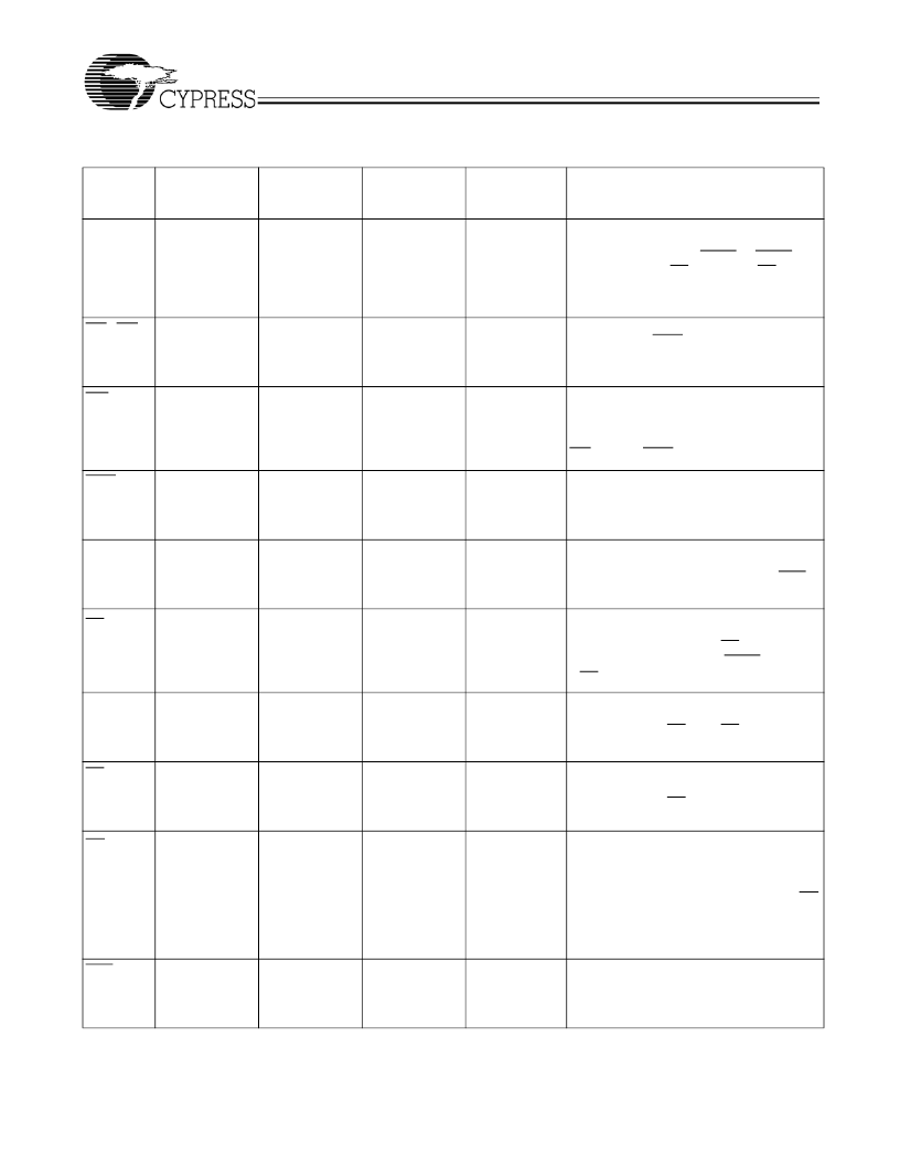
CY7C1383C:Pin Definitions
Name
TQFP
(3-Chip
Enable)
BGA
(1-Chip
Enable)
fBGA
(3-Chip
Enable)
I/O
Description
A
0
, A
1
, A
37,36,32,33,34,
35,42,43,44,45,
46,47,48,49,50,
80,81,82,99,100
P4,N4,A2,B2,
C2,R2,T2,A3,
B3,C3,T3,A5,
B5,C5,T5,A6,
B6,C6,R6,T6
R6,P6,A2,
A10,A11,B2,
B10,N6,P3,P4,
P8,P9,P10,
P11,R3,R4,
R8,R9,R10,R11
Input-
Synchronous
Address Inputs used to select one of the
1M address locations
. Sampled at the ris-
ing edge of the CLK if ADSP or ADSC is
active LOW, and CE
1
,
CE
2
, and
CE
3[2]
are
sampled active. A
[1:0]
feed the 2-bit counter.
BW
A,
BW
B
93,94
L5,G3
B5,A4
Input-
Synchronous
Byte Write Select Inputs, active LOW
.
Qualified with BWE to conduct byte writes
to the SRAM. Sampled on the rising edge of
CLK.
GW
88
H4
B7
Input-
Synchronous
Global Write Enable Input, active LOW
.
When asserted LOW on the rising edge of
CLK, a global write is conducted (ALL bytes
are written, regardless of the values on
BW
[A:B]
and BWE).
BWE
87
M4
A7
Input-
Synchronous
Byte Write Enable Input, active LOW
.
Sampled on the rising edge of CLK. This
signal must be asserted LOW to conduct a
byte write.
CLK
89
K4
B6
Input-
Clock
Clock Input
. Used to capture all
synchronous inputs to the device. Also used
to increment the burst counter when ADV is
asserted LOW, during a burst operation.
CE
1
98
E4
A3
Input-
Synchronous
Chip Enable 1 Input, active LOW
.
Sampled on the rising edge of CLK. Used in
conjunction with CE
2
and CE
3[2]
to
select/deselect the device. ADSP is ignored
if CE
1
is HIGH.
Chip Enable 2 Input, active HIGH
.
Sampled on the rising edge of CLK. Used in
conjunction with CE
1
and CE
3[2]
to
select/deselect the device.
CE
2
97
-
B3
Input-
Synchronous
CE
3[2]
92
-
A6
Input-
Synchronous
Chip Enable 3 Input, active LOW
.
Sampled on the rising edge of CLK. Used in
conjunction with CE
1
and
CE
2
to
select/deselect the device.
Output Enable, asynchronous input,
active LOW
. Controls the direction of the
I/O pins. When LOW, the I/O pins behave as
outputs. When deasserted HIGH, I/O pins
are tri-stated, and act as input data pins. OE
is masked during the first clock of a read
cycle when emerging from a deselected
state.
OE
86
F4
B8
Input-
Asynchronous
ADV
83
G4
A9
Input-
Synchronous
Advance Input signal, sampled on the
rising edge of CLK
. When asserted, it
automatically increments the address in a
burst cycle.
相關(guān)PDF資料 |
PDF描述 |
|---|---|
| CY7C1383C-133AC | CAP .22UF 50V POLY B SERIES |
| CY7C1383C-133BGC | 18-Mb (512K x 36/1M x 18) Flow-Through SRAM |
| CY7C1381D_07 | 18-Mbit (512K x 36/1M x 18) Flow-Through SRAM |
| CY7C1381D-133AXI | 18-Mbit (512K x 36/1M x 18) Flow-Through SRAM |
| CY7C1381D-133BZI | 18-Mbit (512K x 36/1M x 18) Flow-Through SRAM |
相關(guān)代理商/技術(shù)參數(shù) |
參數(shù)描述 |
|---|---|
| CY7C1381C-100BGC | 制造商:Cypress Semiconductor 功能描述: 制造商:Rochester Electronics LLC 功能描述:16MB (512KX36) 3.3V SYNC-FT SRAM - Bulk |
| CY7C1381C-100BGCT | 制造商:Cypress Semiconductor 功能描述: 制造商:Rochester Electronics LLC 功能描述:- Bulk |
| CY7C1381C-100BGI | 制造商:Cypress Semiconductor 功能描述: |
| CY7C1381C-100BZC | 制造商:Cypress Semiconductor 功能描述: |
| CY7C1381C-100BZI | 制造商:Cypress Semiconductor 功能描述: 制造商:Rochester Electronics LLC 功能描述:16MB (512KX36) 3.3V SYNC-FT SRAM - Bulk |
發(fā)布緊急采購,3分鐘左右您將得到回復(fù)。