- 您現(xiàn)在的位置:買賣IC網(wǎng) > PDF目錄223638 > CY7C341B-25RI (CYPRESS SEMICONDUCTOR CORP) UV PLD, 40 ns, CPGA84 PDF資料下載
參數(shù)資料
| 型號(hào): | CY7C341B-25RI |
| 廠商: | CYPRESS SEMICONDUCTOR CORP |
| 元件分類: | PLD |
| 英文描述: | UV PLD, 40 ns, CPGA84 |
| 封裝: | WINDOWED, PGA-84 |
| 文件頁數(shù): | 9/12頁 |
| 文件大小: | 339K |
| 代理商: | CY7C341B-25RI |
USE ULTRA37000 FOR
ALL NEW DESIGNS
CY7C341B
Document #: 38-03016 Rev. *C
Page 6 of 12
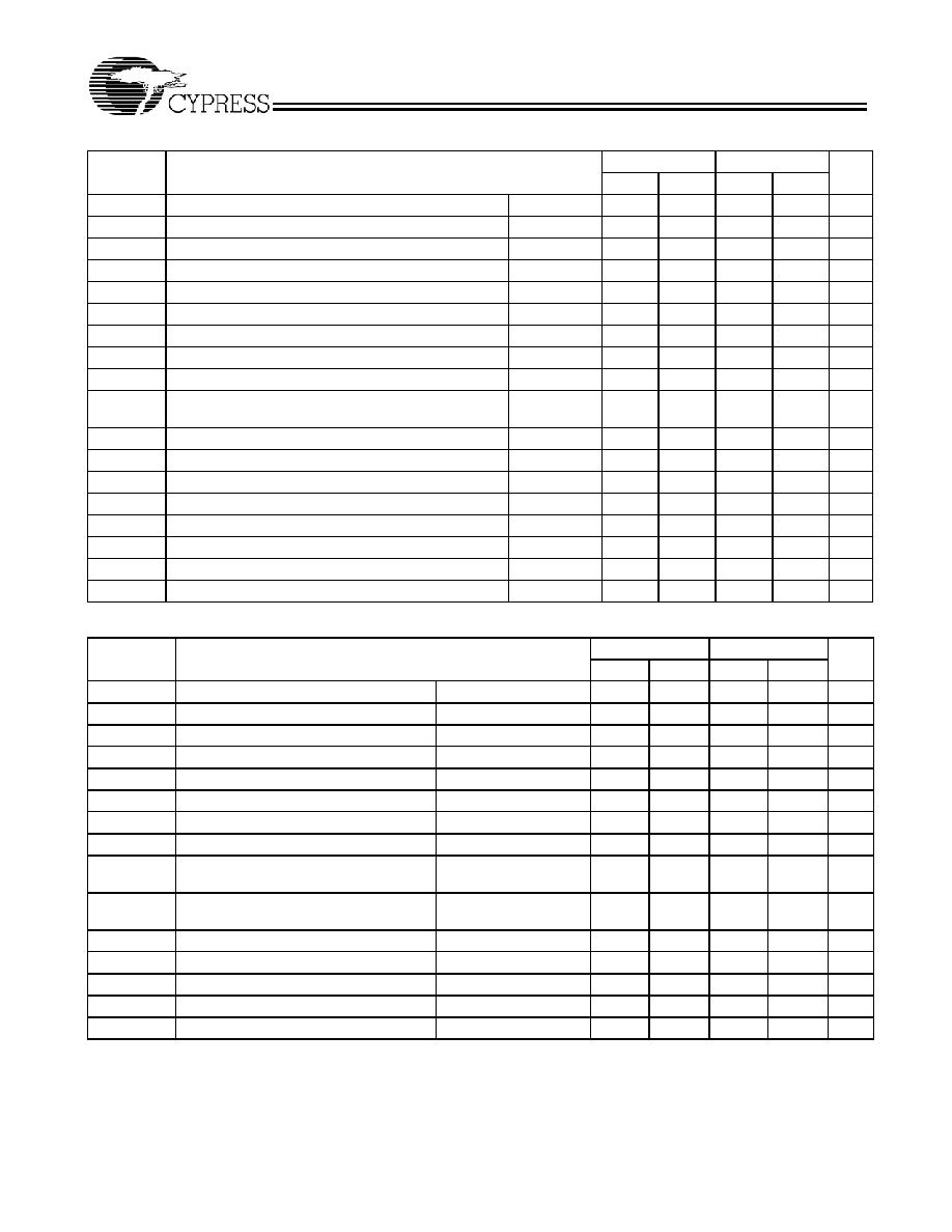
External Switching Characteristics Over the Operating Range
Parameter
Description
7C341B-25
7C341B-35
Unit
Min.
Max.
Min.
Max.
tPD1
Dedicated Input to Combinatorial Output Delay[4]
Commercial
25
35
ns
tPD2
I/O Input to Combinatorial Output Delay[4]
Commercial
40
55
ns
tSU
Global Clock Set-up Time
Commercial
15
25
ns
tCO1
Synchronous Clock Input to Output Delay[4]
Commercial
14
20
ns
tH
Input Hold Time from Synchronous Clock Input
Commercial
0
ns
tWH
Synchronous Clock Input High Time
Commercial
8
12.5
ns
tWL
Synchronous Clock Input Low Time
Commercial
8
12.5
ns
fMAX
Maximum Register Toggle Frequency[5]
Commercial
62.5
40.0
MHz
tACO1
Dedicated Asynchronous Clock Input to Output Delay[4] Commercial
25
35
ns
tAS1
Dedicated Input or Feedback Set-up Time to
Asynchronous Clock Input
Commercial
5
10
ns
tAH
Input Hold Time from Asynchronous Clock Input
Commercial
6
10
ns
tAWH
Asynchronous Clock Input HIGH Time[6]
Commercial
11
16
ns
tAWL
Asynchronous Clock Input LOW Time[6]
Commercial
9
14
ns
tCNT
Minimum Global Clock Period
Commercial
20
30
ns
tODH
Output Data Hold Time After Clock
Commercial
2
ns
fCNT
Maximum Internal Global Clock Frequency[7]
Commercial
50
33.3
MHz
tACNT
Minimum Internal Array Clock Frequency
Commercial
20
30
ns
fACNT
Maximum Internal Array Clock Frequency[7]
Commercial
50
33.3
MHz
Internal Switching Characteristics Over the Operating Range
Parameter
Description
7C341B-25
7C341B-35
Unit
Min.
Max
Min.
Max
tIN
Dedicated Input Pad and Buffer Delay
Commercial
5
11
ns
tIO
I/O Input Pad and Buffer Delay
Commercial
6
11
ns
tEXP
Expander Array Delay
Commercial
12
20
ns
tLAD
Logic Array Data Delay
Commercial
12
14
ns
tLAC
Logic Array Control Delay
Commercial
10
13
ns
tOD
Output Buffer and Pad Delay[4]
Commercial
5
6
ns
tZX
Output Buffer Enable Delay[4]
Commercial
10
13
ns
tXZ
Output Buffer Disable Delay[8]
Commercial
10
13
ns
tRSU
Register Set-Up Time Relative to Clock
Signal at Register
Commercial
6
12
ns
tRH
Register Hold Time Relative to Clock
Signal at Register
Commercial
4
8
ns
tLATCH
Flow-Through Latch Delay
Commercial
3
4
ns
tRD
Register Delay
Commercial
1
2
ns
tCOMB
Transparent Mode Delay
Commercial
3
4
ns
tIC
Asynchronous Clock Logic Delay
Commercial
14
16
ns
tICS
Synchronous Clock Delay
Commercial
3
1
ns
Notes:
4. C1 = 35 pF.
5. The fMAX values represent the highest frequency for pipeline data.
6. This parameter is measured with a positive-edge-triggered clock at the register. For negative-edge clocking, the tACH and tACL parameter must be swapped.
7. This parameter is measured with a 16-bit counter programmed into each LAB.
8. C1 = 5 pF.
相關(guān)PDF資料 |
PDF描述 |
|---|---|
| CY7C341B-35RC | UV PLD, 55 ns, CPGA84 |
| CY7C341B-35RI | UV PLD, 55 ns, CPGA84 |
| CY7C341B-25HC | UV PLD, 40 ns, CQCC84 |
| CY7C341B-25HI | UV PLD, 40 ns, CQCC84 |
| CY7C341B-35HC | UV PLD, 55 ns, CQCC84 |
相關(guān)代理商/技術(shù)參數(shù) |
參數(shù)描述 |
|---|---|
| CY7C341B-35JI | 制造商:Cypress Semiconductor 功能描述:CPLD MAX 制造商:QP Semiconductor 功能描述:7C341B CYP DIE 35NS-PLCC |
| CY7C341B-35RI | 制造商:Cypress Semiconductor 功能描述:CPLD MAX? Family 3.75K Gates 192 Macro Cells 33.3MHz 0.65um Technology 5V 84-Pin Windowed PGA |
| CY7C342-25HC | 制造商:Cypress Semiconductor 功能描述:CMOS EPLD SMD 7C342 PLCC68 5V |
| CY7C342-30HC | 制造商:Cypress Semiconductor 功能描述: 制造商:Cypress Semiconductor 功能描述:Complex Erasable Programmable Logic Device, 128 Cell, 30ns, 68 Pin, Ceramic, PLCC |
| CY7C34235HMB | 制造商:CYPRESS 功能描述:New |
發(fā)布緊急采購,3分鐘左右您將得到回復(fù)。