- 您現(xiàn)在的位置:買賣IC網(wǎng) > PDF目錄369679 > CYNSE70128 Network Processing PDF資料下載
參數(shù)資料
| 型號(hào): | CYNSE70128 |
| 英文描述: | Network Processing |
| 中文描述: | 網(wǎng)絡(luò)處理 |
| 文件頁(yè)數(shù): | 110/126頁(yè) |
| 文件大小: | 3302K |
| 代理商: | CYNSE70128 |
第1頁(yè)第2頁(yè)第3頁(yè)第4頁(yè)第5頁(yè)第6頁(yè)第7頁(yè)第8頁(yè)第9頁(yè)第10頁(yè)第11頁(yè)第12頁(yè)第13頁(yè)第14頁(yè)第15頁(yè)第16頁(yè)第17頁(yè)第18頁(yè)第19頁(yè)第20頁(yè)第21頁(yè)第22頁(yè)第23頁(yè)第24頁(yè)第25頁(yè)第26頁(yè)第27頁(yè)第28頁(yè)第29頁(yè)第30頁(yè)第31頁(yè)第32頁(yè)第33頁(yè)第34頁(yè)第35頁(yè)第36頁(yè)第37頁(yè)第38頁(yè)第39頁(yè)第40頁(yè)第41頁(yè)第42頁(yè)第43頁(yè)第44頁(yè)第45頁(yè)第46頁(yè)第47頁(yè)第48頁(yè)第49頁(yè)第50頁(yè)第51頁(yè)第52頁(yè)第53頁(yè)第54頁(yè)第55頁(yè)第56頁(yè)第57頁(yè)第58頁(yè)第59頁(yè)第60頁(yè)第61頁(yè)第62頁(yè)第63頁(yè)第64頁(yè)第65頁(yè)第66頁(yè)第67頁(yè)第68頁(yè)第69頁(yè)第70頁(yè)第71頁(yè)第72頁(yè)第73頁(yè)第74頁(yè)第75頁(yè)第76頁(yè)第77頁(yè)第78頁(yè)第79頁(yè)第80頁(yè)第81頁(yè)第82頁(yè)第83頁(yè)第84頁(yè)第85頁(yè)第86頁(yè)第87頁(yè)第88頁(yè)第89頁(yè)第90頁(yè)第91頁(yè)第92頁(yè)第93頁(yè)第94頁(yè)第95頁(yè)第96頁(yè)第97頁(yè)第98頁(yè)第99頁(yè)第100頁(yè)第101頁(yè)第102頁(yè)第103頁(yè)第104頁(yè)第105頁(yè)第106頁(yè)第107頁(yè)第108頁(yè)第109頁(yè)當(dāng)前第110頁(yè)第111頁(yè)第112頁(yè)第113頁(yè)第114頁(yè)第115頁(yè)第116頁(yè)第117頁(yè)第118頁(yè)第119頁(yè)第120頁(yè)第121頁(yè)第122頁(yè)第123頁(yè)第124頁(yè)第125頁(yè)第126頁(yè)
CYNSE70032
Document #: 38-02042 Rev. *E
Page 110 of 126
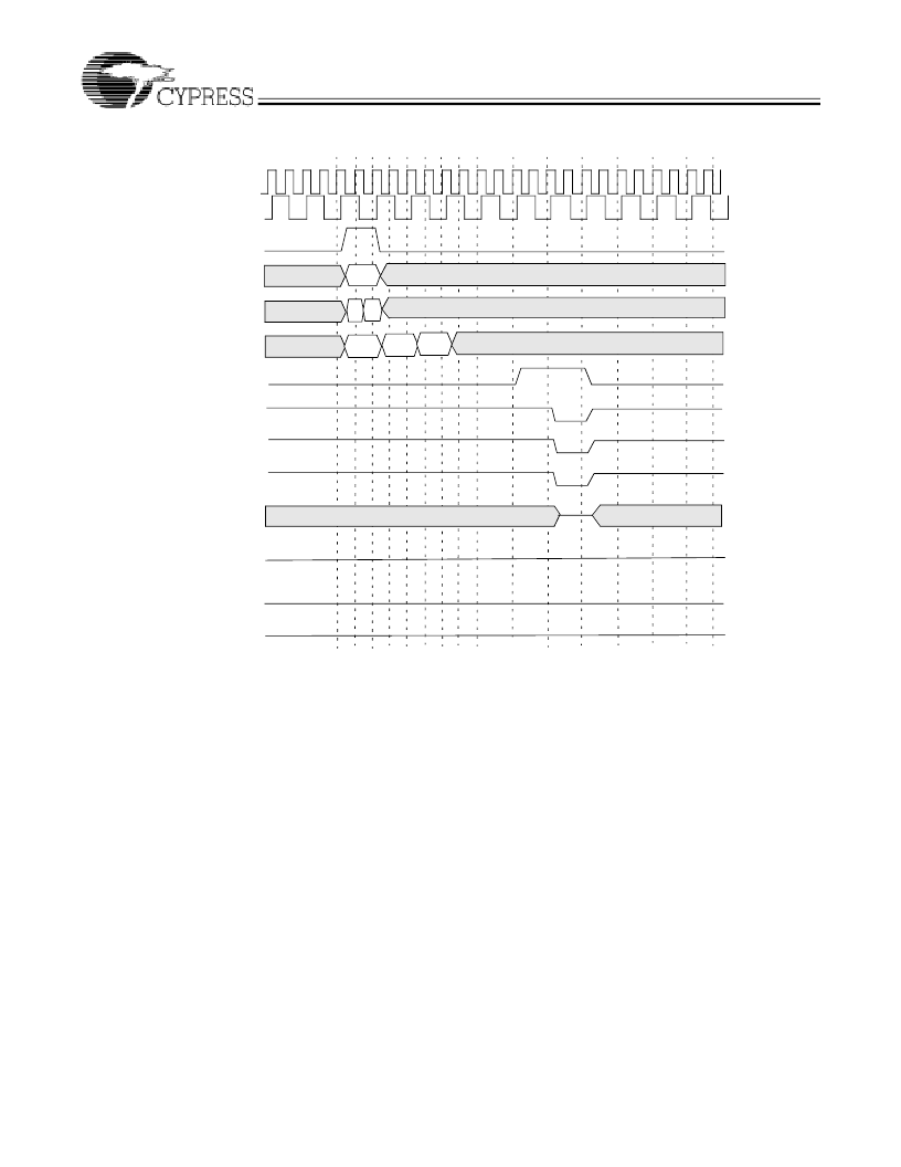
15.8
The following explains the SRAM Write operation done via a table(s) of up to 31 devices and with the following parameters:
TLSZ = 10. The diagram of this table(s) is shown in
Figure 15-12
. The following assumes that SRAM access is accomplished
through CYNSE70032 device number 0 (the selected device).
Figure 15-13
and
Figure 15-14
show the timing diagram for device
number 0 and device number 30, respectively.
Cycle 1A
: The host ASIC applies the Write instruction on CMD[1:0] using CMDV = 1. The DQ bus supplies the address, with
DQ[20:19] set to 10, to select the SRAM address. The host ASIC selects the device for which ID[4:0] matches the DQ[25:21]
lines. The host ASIC also supplies SADR[21:19] on CMD[8:6] in this cycle.
Note
. CMD[2] must be set to 0 for SRAM Write,
because burst Writes into the SRAM are not supported.
Cycle 1B
: The host ASIC continues to apply the Write instruction on CMD[1:0] using CMDV = 1. The DQ bus supplies the
address, with DQ[20:19] set to 10, to select the SRAM address.
Note
. CMD[2] must be set to 0 for SRAM Write, because burst
Write
S
into the SRAM are not supported.
Cycle 2
: The host ASIC continues to drive DQ[67:0]. The data in this cycle is not used by the CYNSE70032.
Cycle 3
: The host ASIC continues to drive DQ[67:0]. The data in this cycle is not used by the CYNSE70032.
At the end of cycle 3, a new command can begin. The Write is a pipelined operation; however, the Write cycle appears at the
SRAM bus with the same latency as the Search instruction (as measured from the second cycle of the Write command).
SRAM Write with Table(s) Consisting of up to 31 Devices
cycle
1
CLK2X
CE_L
cycle
2
cycle
3
cycle
4
cycle
5
cycle
6
cycle
7
cycle
8
cycle
9
cycle
10
PHS_L
SADR[21:0]
SSF
SSV
1
0
0
CMDV
CMD[1:0]
CMD[8:2]
01
Write
A B
Address
DQ
z
WE_L
OE_L
0
ALE_L
z
z
ACK
x
x
1
0
1
1
z
1
1
z
1
TLSZ = 01, HLAT = XXX, LRAM = 1, LDEV = 1
Figure 15-11. SRAM Write Timing for Device Number 7 in a Block of Eight Devices
相關(guān)PDF資料 |
PDF描述 |
|---|---|
| CYNSE70256 | Network Processing |
| CZET101 | Clock Driver |
| CZEU101 | Quad Peripheral Driver |
| CZEZ101 | Triple Peripheral Driver |
| CZSP103 | Voltage Reference |
相關(guān)代理商/技術(shù)參數(shù) |
參數(shù)描述 |
|---|---|
| CYNSE70128-83BGC | 制造商:Cypress Semiconductor 功能描述:NETWORK SEARCH ENGINE 388BGA - Trays |
| CYNSE70128-83BGI | 制造商:Cypress Semiconductor 功能描述:NETWORK SEARCH ENGINE 388BGA - Trays |
| CYNSE70129HV-200BGC | 制造商:Cypress Semiconductor 功能描述: |
| CYNSE70131-250BBC | 制造商:Cypress Semiconductor 功能描述: |
| CYNSE70131A-250BBC | 制造商:Cypress Semiconductor 功能描述: |
發(fā)布緊急采購(gòu),3分鐘左右您將得到回復(fù)。