- 您現在的位置:買賣IC網 > PDF目錄376558 > DAC667 PDF資料下載
參數資料
| 型號: | DAC667 |
| 文件頁數: | 4/9頁 |
| 文件大?。?/td> | 218K |
| 代理商: | DAC667 |
DAC667
4
CS
A3
A2
A1
A0
OPERATION
1
X
0
0
0
0
0
X
1
1
1
1
0
0
X
1
1
1
0
1
0
X
1
1
0
1
1
0
X
1
0
1
1
1
0
No Operation
No Operation
Enable Four LSBs of First Rank
Enable Four Middle Bits of First Rank
Enable Four MSBs of First Rank
Loads Second Rank from First Rank
All Latches Transparent
X = Don’t care.
DISCUSSION OF
SPECIFICATIONS
LINEARITY ERROR
Linearity error is defined as the deviation of the analog
output from a straight line drawn between the end points
(digital inputs all ones and all zeros). DAC667 linearity error
is specified at
±
1/4LSB max at
±
1/2LSB max for J grade.
DIFFERENTIAL LINEARITY ERROR
Differential linearity error (DLE) is the deviation from a
1LSB output change from one adjacent state to the next. A
DLE specification of 1/2LSB means that the output step size
can range from 1/2LSB to 3/2LSB when the digital input
code changes from one code word to the adjacent code word.
If the DLE is more positive than –1LSB, the D/A is said to
be monotonic.
MONOTONICITY
A D/A converter is monotonic if the output either increases
or remains the same for increasing digital input values. The
DAC667 is monotonic over the specification temperature
range.
DRIFT
Gain drift is a measure of the change in the full scale range
(FSR) output over the specification temperature range. Gain
drift is expressed in parts per million per degree Celsius
(ppm/
°
C).
Unipolar offset drift is measured with a data input of
000
HEX
. The D/A is configured for unipolar output. Unipolar
offset drift is expressed in parts per million of full scale
range per degree Celsius (ppm of FSR/
°
C).
Bipolar zero drift is measured with a data input of 800
HEX
.
The D/A is configured for bipolar output. Bipolar zero drift
is expressed in parts per million of full scale range per
degree Celsius (ppm of FSR/
°
C).
SETTLING TIME
Settling time is the total time (including slew time) for the
output to settle to within an error band around its final value
after a change in input. Three settling times are specified to
±
0.01% of full scale range (FSR): two for FSR output
changes of 20V (10k
feedback) and 10V (5k
feedback),
and one for a 1LSB change. The 1LSB change is measured
at the major carry (7FF
HEX
to 800
HEX
, and 800
HEX
to
7FF
HEX
), the input transition at which worst-case settling
time occurs.
OPERATION
DAC667 is a monolithic integrated-circuit 12-bit D/A con-
verter. It is complete with 12-bit D/A switches and ladder
network, voltage reference, output amplifier and micro-
processor bus interface as shown in the front-page diagram.
INTERFACE LOGIC
The bus interface logic of the DAC667 consists of four
independently addressable latches in two ranks. The first
rank consists of three four-bit input latches which can be
loaded directly from a 4-, 8-, 12- or 16-bit microprocessor/
microcontroller bus. These latches hold data temporarily
while a complete 12-bit word is assembled before loading it
into the second rank of latches. This double buffered orga-
nization prevents the generation of spurious analog output
values while the complete word is being assembled.
All latches are level-triggered. Data present when the con-
trol signals are logic 0 will enter the latch. When the control
signals return to logic 1, the data is latched. A truth table for
the control signals is presented in Table I.
It is permissible to enable more than one of the latches
simultaneously. If a first rank latch is enabled coincident
with the second rank latch, the data will reach the second
rank correctly if the timing specifications on page 2 are met.
LOGIC INPUT COMPATIBILITY
The DAC667 digital inputs are TTL compatible (1.4V switch-
ing level) with a low leakage, high input impedance. Thus
the inputs are suitable for being driven by any type of 5V
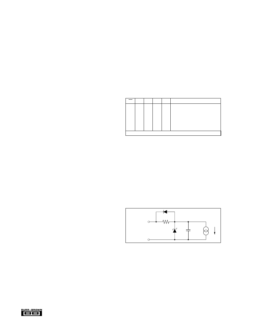
logic. An equivalent circuit of a digital input is shown in
Figure 1.
TABLE I. DAC667 Truth Table.
FIGURE 1. Equivalent Digital Input Circuit.
1k
6.8V
5pF
Digital Input
DCOM
I
I
DAC667 data inputs will float to logic 1 and control inputs
will float to logic 0 if left open. It is recommended that any
unused inputs be connected to power common to improve
noise immunity.
INPUT CODING
The DAC667 accepts positive-true binary input codes.
Input coding for unipolar analog output is straight binary
(USB), where all zeros (000
HEX
) on the data inputs gives a
相關PDF資料 |
PDF描述 |
|---|---|
| DAC667JP | IC-12-BIT DAC |
| DAC701 | Monolithic 16-Bit DIGITAL-TO-ANALOG CONVERTERS |
| DAC702 | Monolithic 16-Bit DIGITAL-TO-ANALOG CONVERTERS |
| DAC703B | Monolithic 16-Bit DIGITAL-TO-ANALOG CONVERTERS |
| DAC703C | Monolithic 16-Bit DIGITAL-TO-ANALOG CONVERTERS |
相關代理商/技術參數 |
參數描述 |
|---|---|
| DAC667AH | 制造商:BURR-BROWN 功能描述: |
| DAC667BH | 制造商:BB 功能描述:_ |
| DAC667JP | 制造商:Rochester Electronics LLC 功能描述:- Bulk 制造商:Texas Instruments 功能描述: |
| DAC667KP | 制造商:Rochester Electronics LLC 功能描述:- Bulk 制造商:BURR-BROWN 功能描述: 制造商:Texas Instruments 功能描述: |
| DAC-6-CG | 制造商:Thomas & Betts 功能描述:2" RIGID TF CONDUIT BODY 制造商:Thomas & Betts 功能描述:Universal Recessed Box And Cover |
發(fā)布緊急采購,3分鐘左右您將得到回復。