- 您現(xiàn)在的位置:買賣IC網 > PDF目錄295418 > DAC7512E/250 (TEXAS INSTRUMENTS INC) SERIAL INPUT LOADING, 8 us SETTLING TIME, 12-BIT DAC, PDSO8 PDF資料下載
參數資料
| 型號: | DAC7512E/250 |
| 廠商: | TEXAS INSTRUMENTS INC |
| 元件分類: | DAC |
| 英文描述: | SERIAL INPUT LOADING, 8 us SETTLING TIME, 12-BIT DAC, PDSO8 |
| 封裝: | GREEN, PLASTIC, MSOP-8 |
| 文件頁數: | 5/23頁 |
| 文件大小: | 1094K |
| 代理商: | DAC7512E/250 |

DAC7512
13
SBAS156B
www.ti.com
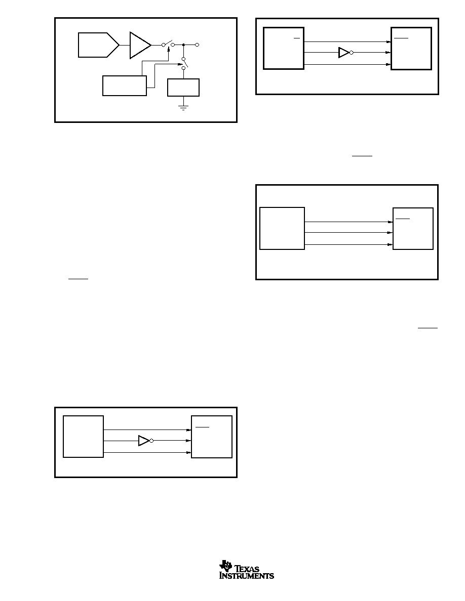
FIGURE 5. Output Stage During Power-Down.
Resistor
String DAC
Amplifier
Power-down
Circuitry
Resistor
Network
V
OUT
All linear circuitry is shut down when the power-down mode
is activated. However, the contents of the DAC register are
unaffected when in power-down. The time to exit power-
down is typically 2.5s for VDD = 5V and 5s for VDD = 3V.
See the Typical Characteristics for more information.
MICROPROCESSOR
INTERFACING
DAC7512 TO 8051 INTERFACE
Figure 6 shows a serial interface between the DAC7512 and
a typical 8051-type microcontroller. The setup for the inter-
face is as follows: TXD of the 8051 drives SCLK of the
DAC7512, while RXD drives the serial data line of the part.
The SYNC signal is derived from a bit programmable pin on
the port. In this case, port line P3.3 is used. When data is to
be transmitted to the DAC7512, P3.3 is taken LOW. The
8051 transmits data only in 8-bit bytes; thus only eight falling
clock edges occur in the transmit cycle. To load data to the
DAC, P3.3 is left LOW after the first eight bits are transmitted,
and a second write cycle is initiated to transmit the second
byte of data. P3.3 is taken HIGH following the completion of
this cycle. The 8051 outputs the serial data in a format which
has the LSB first. The DAC7512 requires its data with the
MSB as the first bit received. The 8051 transmit routine must
therefore take this into account, and “mirror” the data as
needed.
FIGURE 6. DAC7512 to 80C51/80L51 Interface.
80C51/80L51(1)
P3.3
TXD
RXD
DAC7512(1)
SYNC
SCLK
D
IN
NOTE: (1) Additional pins omitted for clarity.
FIGURE 7. DAC7512 to Microwire Interface.
SYNC
SCLK
D
IN
MicrowireTM
CS
SK
SO
DAC7513(1)
NOTE: (1) Additional pins omitted for clarity.
Microwire is a registered trademark of National Semiconductor.
DAC7512 TO 68HC11 INTERFACE
Figure 8 shows a serial interface between the DAC7512 and
the 68HC11 microcontroller. SCK of the 68HC11 drives the
SCLK of the DAC7512, while the MOSI output drives the
serial data line of the DAC. The SYNC signal is derived from
a port line (PC7), similar to what was done for the 8051.
FIGURE 8. DAC7512 to 68HC11 Interface.
68HC11(1)
PC7
SCK
MOSI
SYNC
SCLK
D
IN
DAC7513(1)
NOTE: (1) Additional pins omitted for clarity.
The 68HC11 should be configured so that its CPOL bit is a
0 and its CPHA bit is a 1. This configuration causes data
appearing on the MOSI output is valid on the falling edge of
SCK. When data is being transmitted to the DAC, the SYNC
line is taken LOW (PC7). Serial data from the 68HC11 is
transmitted in 8-bit bytes with only eight falling clock edges
occurring in the transmit cycle. Data is transmitted MSB first.
In order to load data to the DAC7512, PC7 is left LOW after
the first eight bits are transferred, and a second serial write
operation is performed to the DAC and PC7 is taken HIGH
at the end of this procedure.
APPLICATIONS
USING REF02 AS A POWER
SUPPLY FOR THE DAC7512
Due to the extremely low supply current required by the
DAC7512, an alternative option is to use a REF02 +5V
precision voltage reference to supply the required voltage to
the part, see Figure 9. This is especially useful if the power
supply is too noisy or if the system supply voltages are at
some value other than 5V. The REF02 will output a steady
supply voltage for the DAC7512. If the REF02 is used, the
current it needs to supply to the DAC7512 is 135A. This is
with no load on the output of the DAC. When the DAC output
DAC7512 TO MICROWIRE INTERFACE
Figure 7 shows an interface between the DAC7512 and any
Microwire compatible device. Serial data is shifted out on the
falling edge of the serial clock and is clocked into the
DAC7512 on the rising edge of the SK signal.
相關PDF資料 |
PDF描述 |
|---|---|
| DAC7512N/3K | SERIAL INPUT LOADING, 8 us SETTLING TIME, 12-BIT DAC, PDSO6 |
| DAC7631EB | SERIAL INPUT LOADING, 8 us SETTLING TIME, 16-BIT DAC, PDSO20 |
| DAC7631E | SERIAL INPUT LOADING, 8 us SETTLING TIME, 16-BIT DAC, PDSO20 |
| DAC7631E/1KG4 | SERIAL INPUT LOADING, 8 us SETTLING TIME, 16-BIT DAC, PDSO20 |
| DAC8830IBDG4 | SERIAL INPUT LOADING, 1 us SETTLING TIME, 16-BIT DAC, PDSO8 |
相關代理商/技術參數 |
參數描述 |
|---|---|
| DAC7512N | 制造商:Texas Instruments 功能描述: |
| DAC7512N/250 | 功能描述:數模轉換器- DAC Lo-Pwr R-To-R Output 12-Bit Serial Input RoHS:否 制造商:Texas Instruments 轉換器數量:1 DAC 輸出端數量:1 轉換速率:2 MSPs 分辨率:16 bit 接口類型:QSPI, SPI, Serial (3-Wire, Microwire) 穩(wěn)定時間:1 us 最大工作溫度:+ 85 C 安裝風格:SMD/SMT 封裝 / 箱體:SOIC-14 封裝:Tube |
| DAC7512N/250G4 | 功能描述:數模轉換器- DAC Lo-Pwr R-To-R Output 12-Bit Serial Input RoHS:否 制造商:Texas Instruments 轉換器數量:1 DAC 輸出端數量:1 轉換速率:2 MSPs 分辨率:16 bit 接口類型:QSPI, SPI, Serial (3-Wire, Microwire) 穩(wěn)定時間:1 us 最大工作溫度:+ 85 C 安裝風格:SMD/SMT 封裝 / 箱體:SOIC-14 封裝:Tube |
| DAC7512N/3K | 功能描述:數模轉換器- DAC Lo-Pwr R-To-R Output 12-Bit Serial Input RoHS:否 制造商:Texas Instruments 轉換器數量:1 DAC 輸出端數量:1 轉換速率:2 MSPs 分辨率:16 bit 接口類型:QSPI, SPI, Serial (3-Wire, Microwire) 穩(wěn)定時間:1 us 最大工作溫度:+ 85 C 安裝風格:SMD/SMT 封裝 / 箱體:SOIC-14 封裝:Tube |
| DAC7512N/3KG4 | 功能描述:數模轉換器- DAC Lo-Pwr R-To-R Output 12-Bit Serial Input RoHS:否 制造商:Texas Instruments 轉換器數量:1 DAC 輸出端數量:1 轉換速率:2 MSPs 分辨率:16 bit 接口類型:QSPI, SPI, Serial (3-Wire, Microwire) 穩(wěn)定時間:1 us 最大工作溫度:+ 85 C 安裝風格:SMD/SMT 封裝 / 箱體:SOIC-14 封裝:Tube |
發(fā)布緊急采購,3分鐘左右您將得到回復。