- 您現(xiàn)在的位置:買賣IC網(wǎng) > PDF目錄376562 > DAC8012JU-BI 12-Bit Digital-to-Analog Converter PDF資料下載
參數(shù)資料
| 型號: | DAC8012JU-BI |
| 英文描述: | 12-Bit Digital-to-Analog Converter |
| 中文描述: | 12位數(shù)字到模擬轉(zhuǎn)換器 |
| 文件頁數(shù): | 5/9頁 |
| 文件大小: | 211K |
| 代理商: | DAC8012JU-BI |

5
DAC80/80P
DISCUSSION OF
SPECIFICATIONS
DIGITAL INPUT CODES
The DAC80 accepts complementary binary digital input
codes. The CBI model may be connected by the user for any
one of three complementary codes: CSB, COB, or CTC (see
Table I).
ACCURACY
Linearity of a D/A converter is the true measure of its
performance. The linearity error of the DAC80 is specified
over its entire temperature range. This means that the analog
output will not vary by more than
±
1/2LSB, maximum, from
an ideal straight line drawn between the end points (inputs
all “1”s and all “0”s) over the specified temperature range of
0
°
C to +70
°
C.
Differential linearity error of a D/A converter is the devia-
tion from an ideal 1LSB voltage change from one adjacent
output state to the next. A differential linearity error speci-
fication of
±
1/2LSB means that the output voltage step sizes
can range from 1/2LSB to 3/2LSB when the input changes
from one adjacent input state to the next.
Monotonicity over a 0
°
C to +70
°
C range is guaranteed in the
DAC80 to insure that the analog output will increase or
remain the same for increasing input digital codes.
DRIFT
Gain Drift is a measure of the change in the full scale range
output over temperature expressed in parts per million per
°
C (ppm/
°
C). Gain drift is established by: 1) testing the end
point differences for each DAC80 model at 0
°
C, +25
°
C, and
+70
°
C; 2) calculating the gain error with respect to the 25
°
C
value, and; 3) dividing by the temperature change. This
figure is expressed in ppm/
°
C and is given in the electrical
specifications both with and without internal reference.
Offset Drift is a measure of the actual change in output with
all “1”s on the input over the specified temperature range.
The offset is measured at 0
°
C, +25
°
C, and 70
°
C. The
maximum change in Offset is referenced to the Offset at
25
°
C and is divided by the temperature range. This drift is
expressed in parts per million of full scale range per
°
C (ppm
of FSR/
°
C).
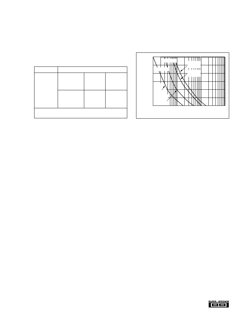
SETTLING TIME
Settling time for each DAC80 model is the total time
(including slew time) required for the output to settle within
an error band around its final value after a change in input
(see Figure 1).
Voltage Output Models
Three settling times are specified to
±
0.01% of full scale
range (FSR); two for maximum full scale range changes of
20V, 10V and one for a 1LSB change. The 1LSB change is
measured at the major carry (0111...11 to 1000...00), the
point at which the worst case settling time occurs.
Current Output Models
Two settling times are specified to
±
0.01% of FSR. Each is
given for current models connected with two different resis-
tive loads: 10
to 100
and 1000
to 1875
. Internal
resistors are provided for connecting nominal load resis-
tances of approximately 1000
to 1800
for output voltage
range of
±
1V and 0 to –2V (see Figures 11 and 12).
COMPLIANCE
Compliance voltage is the maximum voltage swing allowed
on the current output node in order to maintain specified
accuracy. The maximum compliance voltage of all current
output models is
±
2.5V. Maximum safe voltage range of
±
1V and 0 to –2V (see Figures 11 and 12).
POWER SUPPLY SENSITIVITY
Power supply sensitivity is a measure of the effect of a
power supply change on the D/A converter output. It is
defined as a percent of FSR per percent of change in either
the positive or negative supplies about the nominal power
supply voltages (see Figure 2).
REFERENCE SUPPLY
All DAC80 models are supplied with an internal 6.3V
reference voltage supply. This voltage (pin 24) has a toler-
ance of
±
1% and must be connected to the Reference Input
DIGITAL INPUT
ANALOG OUTPUT
CSB
COB
CTC
(1)
Complementary
Straight
Binary
Complementary
Offset
Binary
Complementary
Two’s
Complement
MSB
↓
LSB
↓
000000000000
011111111111
100000000000
111111111111
+Full Scale
+1/2 Full Scale
1/2 Full Scale –1LSB
Zero
+Full Scale
Zero
–1LSB
–Full Scale
–1LSB
–Full Scale
–Full Scale
Zero
NOTE: (1) Invert the MSB of the COB code with an external inverter to obtain
CTC code.
TABLE I. Digital Input Codes.
FIGURE 1. Full Scale Range Settling Time vs Accuracy.
0.1
Settling Time (μs)
1
10
100
A
P
1
0.3
0.1
0.03
0.01
0.003
0.001
R
L
=
10
to 100
R
=
1000
to 1875
10k
Feedback
5k
Feedback
V Models
I Models
相關(guān)PDF資料 |
PDF描述 |
|---|---|
| DAC8043AFP | 12-Bit Serial Input Multiplying D/A Converter |
| DAC8043AFRU | 12-Bit Serial Input Multiplying D/A Converter |
| DAC8043A | 12-Bit Serial Input Multiplying D/A Converter |
| DAC8043AFS | 12-Bit Serial Input Multiplying D/A Converter |
| DAC8043AEP | 12-Bit Serial Input Multiplying D/A Converter |
相關(guān)代理商/技術(shù)參數(shù) |
參數(shù)描述 |
|---|---|
| DAC8012KU-BI | 制造商:未知廠家 制造商全稱:未知廠家 功能描述:12-Bit Digital-to-Analog Converter |
| DAC802 | 制造商:NSC 制造商全稱:National Semiconductor 功能描述:8 BIT DIGITAL TO ANALOG CONVERTERS |
| DAC8043 | 制造商:BB 制造商全稱:BB 功能描述:CMOS 12-Bit Serial Input Multiplying DIGITAL-TO-ANALOG CONVERTER |
| DAC8043A | 制造商:AD 制造商全稱:Analog Devices 功能描述:12-Bit Serial Input Multiplying D/A Converter |
| DAC8043A1ES | 功能描述:IC DAC 12BIT MULT SRL INP 8-SOIC RoHS:否 類別:集成電路 (IC) >> 數(shù)據(jù)采集 - 數(shù)模轉(zhuǎn)換器 系列:- 標準包裝:2,400 系列:- 設(shè)置時間:- 位數(shù):18 數(shù)據(jù)接口:串行 轉(zhuǎn)換器數(shù)目:3 電壓電源:模擬和數(shù)字 功率耗散(最大):- 工作溫度:-40°C ~ 85°C 安裝類型:表面貼裝 封裝/外殼:36-TFBGA 供應(yīng)商設(shè)備封裝:36-TFBGA 包裝:帶卷 (TR) 輸出數(shù)目和類型:* 采樣率(每秒):* |
發(fā)布緊急采購,3分鐘左右您將得到回復(fù)。