- 您現(xiàn)在的位置:買賣IC網(wǎng) > PDF目錄1911 > DG3517DB-T5-E1 (Vishay Siliconix)IC SWITCH DUAL SPDT 10MICRO PDF資料下載
參數(shù)資料
| 型號: | DG3517DB-T5-E1 |
| 廠商: | Vishay Siliconix |
| 文件頁數(shù): | 4/11頁 |
| 文件大?。?/td> | 0K |
| 描述: | IC SWITCH DUAL SPDT 10MICRO |
| 標準包裝: | 3,000 |
| 功能: | 開關(guān) |
| 電路: | 2 x SPDT - NC/NO |
| 導(dǎo)通狀態(tài)電阻: | 2.9 歐姆 |
| 電壓電源: | 單電源 |
| 電壓 - 電源,單路/雙路(±): | 1.8 V ~ 5.5 V |
| 電流 - 電源: | 1µA |
| 工作溫度: | -40°C ~ 85°C |
| 安裝類型: | 表面貼裝 |
| 封裝/外殼: | 10-WFBGA |
| 供應(yīng)商設(shè)備封裝: | 10-Micro Foot?(4x3) |
| 包裝: | 帶卷 (TR) |
www.vishay.com
2
Document Number: 73404
S11-1185-Rev. D, 13-Jun-11
Vishay Siliconix
DG3516, DG3517
This document is subject to change without notice.
THE PRODUCTS DESCRIBED HEREIN AND THIS DOCUMENT ARE SUBJECT TO SPECIFIC DISCLAIMERS, SET FORTH AT www.vishay.com/doc?91000
Product is End of Life
Notes:
a. Signals on NC, NO, or COM or IN exceeding V+ will be clamped by internal diodes. Limit forward diode current to maximum current ratings.
b. Refer to IPC/JEDEC (J-STD-020B).
c. All bumps welded or soldered to PC board.
d. Derate 5.7 mW/°C above 70 °C.
Stresses beyond those listed under “Absolute Maximum Ratings” may cause permanent damage to the device. These are stress ratings only, and functional operation
of the device at these or any other conditions beyond those indicated in the operational sections of the specifications is not implied. Exposure to absolute maximum
rating conditions for extended periods may affect device reliability.
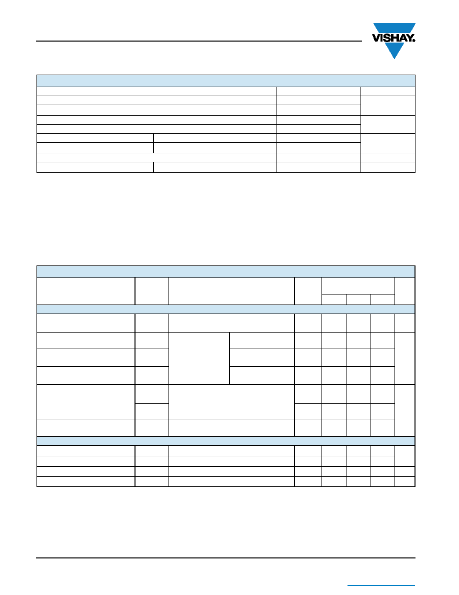
ABSOLUTE MAXIMUM RATINGS
Parameter
Limit
Unit
Reference V+ to GND
- 0.3 to + 6
V
IN, COM, NC, NOa
- 0.3 to (V+ + 0.3)
Continuous Current (NO, NC, COM)
± 100
mA
Peak Current (Pulsed at 1 ms, 10 % duty cycle)
± 200
Storage Temperature
(D Suffix)
- 65 to 150
°C
Package Solder Reflow Conditionsb
IR/Convection
250
ESD per Method 3015.7
> 2
kV
Power Dissipation (Packages)c
MICRO FOOT: 10 Bump (4 mm x 3 mm)d
457
mW
SPECIFICATIONS (V+ = 3 V)
Parameter
Symbol
Test Conditions
Otherwise Unless Specified
V+ = 2.7 V to 3.6 V, VIN = 0.5 V or 1.4 V
e
Temp.a
Limits
- 40 °C to 85 °C
Unit
Min.b
Typ.c
Max.b
Analog Switch
Analog Signal Ranged
VNO, VNC,
VCOM
Full
0
V+
V
On-Resistanced
RON
V+ = 2.7 V
INO, INC = 10 mA
VCOM = 1.5 V
Room
Full
2.5
3.5
3.8
Ω
RON Flatness
d
RON
Flatness
VCOM = 1, 1.5, 2 V
Room
0.52
1
On-Resistance
Match Between Channelsd
ΔRDS(on)
VCOM = 1.5 V
Room
0.25
Switch Off Leakage Current
INO(off)
INC(off)
V+ = 3.3 V,
VNO, VNC = 0.3 V/3 V, VCOM = 3 V/0.3 V
Room
Full
- 2
- 20
2
20
nA
ICOM(off)
Room
Full
- 2
- 20
2
20
Channel-On Leakage Current
ICOM(on)
V+ = 3.3 V, VNO, VNC = VCOM = 0.3 V/3 V
Room
Full
- 2
- 20
2
20
Digital Control
Input High Voltaged
VINH
Full
1.4
V
Input Low Voltage
VINL
Full
0.5
Input Capacitance
Cin
Full
5
pF
Input Current
IINL or IINH
VIN = 0 V or V+
Full
1
A
相關(guān)PDF資料 |
PDF描述 |
|---|---|
| DG3536DB-T5-E1 | IC SWITCH DUAL SPDT 10MICRO |
| DG3539DB-T5-E1 | IC SWITCH DUAL SPDT 8MICRO |
| DG384BDJ-E3 | IC SWITCH DUAL DPST 16DIP |
| DG387ACJ | IC SWITCH SPDT 14DIP |
| DG403BDJ-E3 | IC ANALOG SWITCH SPDT 16DIP |
相關(guān)代理商/技術(shù)參數(shù) |
參數(shù)描述 |
|---|---|
| DG3520A02XX_D5X WAF | 制造商:Fairchild Semiconductor Corporation 功能描述: |
| DG3520X01XX-D4X WAF | 制造商:Fairchild Semiconductor Corporation 功能描述: |
| DG3530X01XX_D4X WAF | 制造商:Fairchild Semiconductor Corporation 功能描述: |
| DG3535 | 制造商:VISHAY 制造商全稱:Vishay Siliconix 功能描述:0.25ohm Low-Voltage Dual SPDT Analog Switch |
| DG3535_08 | 制造商:VISHAY 制造商全稱:Vishay Siliconix 功能描述:0.25-Ω Low-Voltage Dual SPDT Analog Switch |
發(fā)布緊急采購,3分鐘左右您將得到回復(fù)。