- 您現(xiàn)在的位置:買賣IC網(wǎng) > PDF目錄171212 > DP83957 PDF資料下載
參數(shù)資料
| 型號(hào): | DP83957 |
| 文件頁數(shù): | 23/24頁 |
| 文件大小: | 240K |
| 代理商: | DP83957 |
50 Functional Description (Continued)
513 SRAM Write Operation
A write to the SRAM can occur due to a CPU request to one
or all of the MIB attributes or due to normal updating of
attributes by the DP83957 after receiving the management
status bytes from a DP83950
In the latter case the access to the SRAM is done automati-
cally by the DP83957 In the case of a CPU request the
SRAM address must be specified in the same manner as
the read operation (refer to Section 512)
The DP83957 can write data to the SRAM one byte at a
time or it can fill the entire SRAM with the same value The
value to be written into the SRAM is specified in the Write
Data Byte register
The CPU initiates a one-byte SRAM write by setting the
ST
WR bit (D5) in Configuration Register 1
In order to fill the entire SRAM both the FILL (D3) and the
ST
WR (D5) bits must be set in Configuration Register 1
This fill-mode is used to initialize the SRAM to a common
value For example reset all the attributes to zero
The DP83957 indicates the completion of the SRAM write
operation by sending an interrupt (if enabled) to the CPU
and setting the WR
COM bit (D5) in the Interrupt Status
Register
514 SRAM Memory Map
The memory map for the DP83957 consists of two sections
Each section represents one DP83950 device as shown in
the SRAM Memory Map
For each DP83950 the map is further divided into 13 pages
where each page represents a physical port for the
DP83950 The DP83950 ID and Port number selection is
programmed into Access 2 Register
Each port page is further sub-divided into 64 locations
These locations represent the offset of the Port’s Attributes
This offset is programmed into Access 1 Register
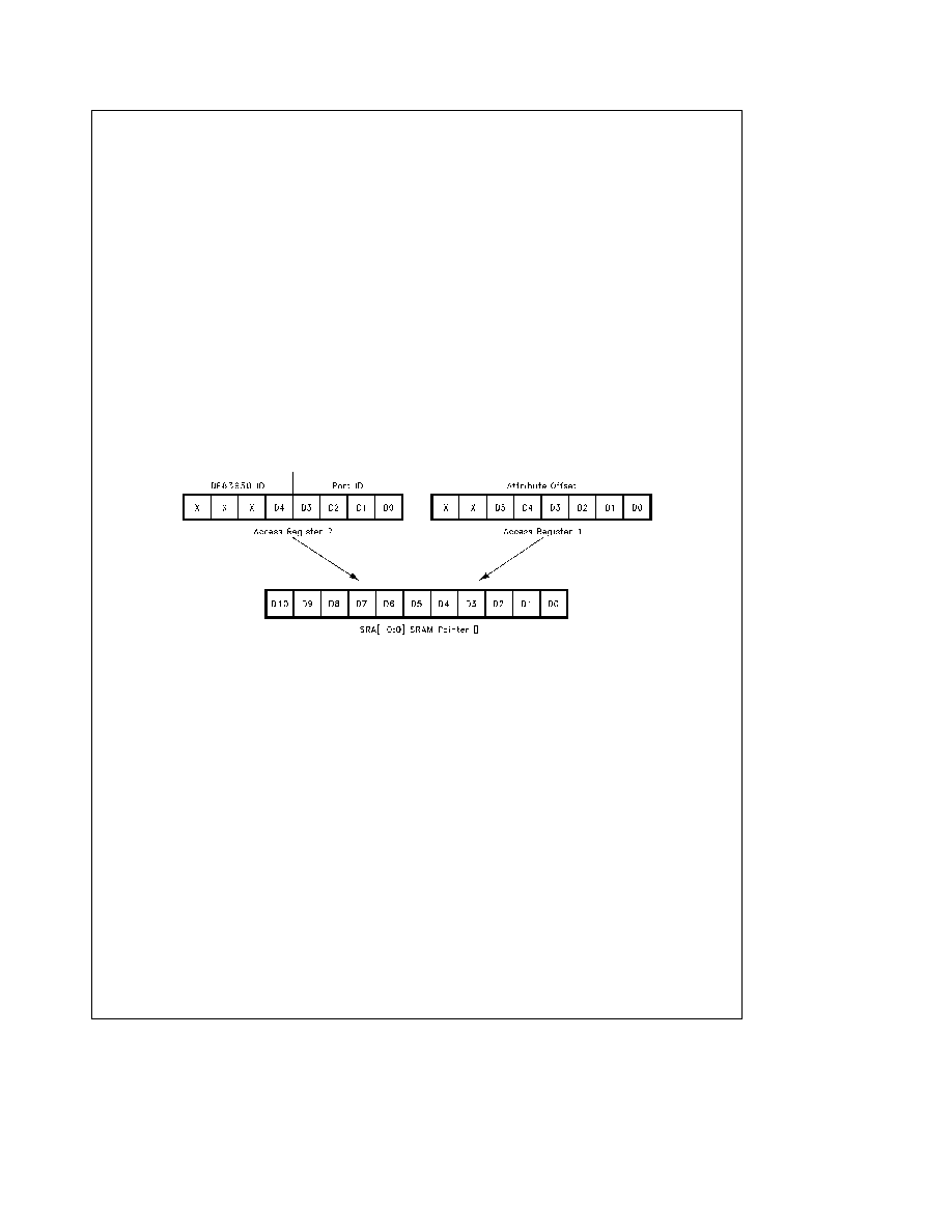
515 SRAM Address Format
The SRAM SRA 100 address is made up by combining the
contents of Access Registers 1 and 2 This is shown in the
SRAM Address Pointer figure below
SRAM Address Pointer
TLF12437 – 5
8
相關(guān)PDF資料 |
PDF描述 |
|---|---|
| DP83957VF | REPEATER MANAGEMENT|QFP|80PIN|PLASTIC |
| DP83959AVUL | LAN Hub Controller |
| DP83BC04BJ | Single 8-bit Bus Transceiver |
| DP83BC04BN | Single 8-bit Bus Transceiver |
| DP8400-2 | Error Detection & Correction (EDAC) |
相關(guān)代理商/技術(shù)參數(shù) |
參數(shù)描述 |
|---|---|
| DP83957VF | 制造商:未知廠家 制造商全稱:未知廠家 功能描述:REPEATER MANAGEMENT|QFP|80PIN|PLASTIC |
| DP83959 | 制造商:NSC 制造商全稱:National Semiconductor 功能描述:8-Port Lite Ethernet Repeater Interface Controller |
| DP83959AVUL | 制造商:未知廠家 制造商全稱:未知廠家 功能描述:LAN Hub Controller |
| DP83959VUL | 制造商:NSC 制造商全稱:National Semiconductor 功能描述:8-Port Lite Ethernet Repeater Interface Controller |
| DP83BC04BJ | 制造商:未知廠家 制造商全稱:未知廠家 功能描述:Single 8-bit Bus Transceiver |
發(fā)布緊急采購,3分鐘左右您將得到回復(fù)。