- 您現(xiàn)在的位置:買賣IC網(wǎng) > PDF目錄362580 > E28F160S5-100 (INTEL CORP) 16 Characters x 2 Lines, 5x7 Dot Matrix Character and Cursor PDF資料下載
參數(shù)資料
| 型號(hào): | E28F160S5-100 |
| 廠商: | INTEL CORP |
| 元件分類: | PROM |
| 英文描述: | 16 Characters x 2 Lines, 5x7 Dot Matrix Character and Cursor |
| 中文描述: | 2M X 8 FLASH 5V PROM, 100 ns, PDSO56 |
| 封裝: | 14 X 20 MM, TSOP-56 |
| 文件頁(yè)數(shù): | 10/50頁(yè) |
| 文件大?。?/td> | 1220K |
| 代理商: | E28F160S5-100 |
第1頁(yè)第2頁(yè)第3頁(yè)第4頁(yè)第5頁(yè)第6頁(yè)第7頁(yè)第8頁(yè)第9頁(yè)當(dāng)前第10頁(yè)第11頁(yè)第12頁(yè)第13頁(yè)第14頁(yè)第15頁(yè)第16頁(yè)第17頁(yè)第18頁(yè)第19頁(yè)第20頁(yè)第21頁(yè)第22頁(yè)第23頁(yè)第24頁(yè)第25頁(yè)第26頁(yè)第27頁(yè)第28頁(yè)第29頁(yè)第30頁(yè)第31頁(yè)第32頁(yè)第33頁(yè)第34頁(yè)第35頁(yè)第36頁(yè)第37頁(yè)第38頁(yè)第39頁(yè)第40頁(yè)第41頁(yè)第42頁(yè)第43頁(yè)第44頁(yè)第45頁(yè)第46頁(yè)第47頁(yè)第48頁(yè)第49頁(yè)第50頁(yè)
28F160S5, 28F320S5
E
10
ADVANCE INFORMATION
Read Array, Status Register, query, and identifier
codes can be accessed through the CUI
independent
of
the
programming voltage on V
PP
enables successful
block
erasure,
program,
configuration. All functions associated with
altering memory contents
—block erase, program,
lock-bit configuration, status, and identifier
codes—are accessed via the CUI and verified
through the Status Register.
V
PP
voltage.
Proper
and
lock-bit
Commands are written using standard micro-
processor write timings. The CUI contents serve
as input to the WSM that controls the block
erase, programming, and lock-bit configuration.
The internal algorithms are regulated by the
WSM,
including
pulse
verification, and margining of data. Addresses
and data are internally latched during write
cycles. Writing the appropriate command outputs
array data, identifier codes, or Status Register
data.
repetition,
internal
Interface software that initiates and polls
progress of block erase, programming, and lock-
bit configuration can be stored in any block. This
code is copied to and executed from system
RAM during flash memory updates. After
successful completion, reads are again possible
via the Read Array command. Block erase
suspend allows system software to suspend a
block erase to read or write data from any other
block. Program suspend allows system software
to suspend a program to read data from any
other flash memory array location.
2.1
Data Protection
Depending on the application, the system
designer may choose to make the V
PP
power
supply switchable or hardwired to V
PPH
. The
device supports either design practice, and
encourages optimization of the processor-
memory interface.
When V
PP
≤
V
PPLK
, memory contents cannot be
altered. When high voltage is applied to V
PP
, the
two-step block erase, program, or lock-bit
configuration
command
protection from unwanted operations. All write
functions are disabled when V
CC
voltage is below
the write lockout voltage V
LKO
or when RP# is at
V
IL
. The device’s block locking capability
provides additional protection from inadvertent
code or data alteration.
sequences
provide
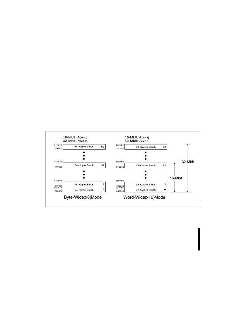
0608_05
Figure 4. Memory Map
相關(guān)PDF資料 |
PDF描述 |
|---|---|
| E28F320S5-110 | 16 Characters x 2 Lines, 5x7 Dot Matrix Character and Cursor |
| E28F160S5-70 | 16 Characters x 2 Lines, 5x7 Dot Matrix Character and Cursor |
| E28F320S5-90 | 16 Characters x 2 Lines, 5x7 Dot Matrix Character and Cursor |
| E28F200CVB60 | 2-MBIT SmartVoltage BOOT BLOCK FLASH MEMORY FAMILY |
| E28F200BVB60 | 2-MBIT SmartVoltage BOOT BLOCK FLASH MEMORY FAMILY |
相關(guān)代理商/技術(shù)參數(shù) |
參數(shù)描述 |
|---|---|
| E28F160S5-70 | 制造商:INTEL 制造商全稱:Intel Corporation 功能描述:WORD-WIDE FlashFile MEMORY FAMILY |
| E28F200B5B60 | 制造商:INTEL 制造商全稱:Intel Corporation 功能描述:SMART 5 BOOT BLOCK FLASH MEMORY FAMILY 2, 4, 8 MBIT |
| E28F200B5B80 | 制造商:INTEL 制造商全稱:Intel Corporation 功能描述:SMART 5 BOOT BLOCK FLASH MEMORY FAMILY 2, 4, 8 MBIT |
| E28F200B5T60 | 制造商:INTEL 制造商全稱:Intel Corporation 功能描述:SMART 5 BOOT BLOCK FLASH MEMORY FAMILY 2, 4, 8 MBIT |
| E28F200B5T80 | 制造商:Rochester Electronics LLC 功能描述:- Bulk 制造商:Intel 功能描述: |
發(fā)布緊急采購(gòu),3分鐘左右您將得到回復(fù)。