- 您現在的位置:買賣IC網 > PDF目錄295878 > EL7642AILTZ-T13 (INTERSIL CORP) TFT-LCD DC/DC with Integrated Amplifiers PDF資料下載
參數資料
| 型號: | EL7642AILTZ-T13 |
| 廠商: | INTERSIL CORP |
| 元件分類: | 穩(wěn)壓器 |
| 英文描述: | TFT-LCD DC/DC with Integrated Amplifiers |
| 中文描述: | 0.15 A SWITCHING REGULATOR, 1350 kHz SWITCHING FREQ-MAX, QCC32 |
| 封裝: | 5 X 5 MM, ROHS COMPLIANT, MO-220, QFN-32 |
| 文件頁數: | 6/19頁 |
| 文件大小: | 458K |
| 代理商: | EL7642AILTZ-T13 |
14
FN6270.0
May 15, 2006
Calculation of the Linear Regulator Base-emitter
Resistors (RBP and RBN)
For the pass transistor of the linear regulator, low frequency
gain (Hfe) and unity gain frequency (fT) are usually specified
in the datasheet. The pass transistor adds a pole to the loop
transfer function at fp = fT/Hfe. Therefore, in order to
maintain phase margin at low frequency, the best choice for
a pass device is often a high frequency low gain switching
transistor. Further improvement can be obtained by adding a
base-emitter resistor RBE (RBP, RBL, RBN in the Functional
Block Diagram), which increases the pole frequency to:
fp = fT*(1+ Hfe *re/RBE)/Hfe, where re = KT/qIc. So choose
the lowest value RBE in the design as long as there is still
enough base current (IB) to support the maximum output
current (IC).
We will take as an example the VON linear regulator. If a
Fairchild MMBT3906 PNP transistor is used as the external
pass transistor, Q11 in the application diagram, then for a
maximum VON operating requirement of 50mA the data
sheet indicates Hfe_min = 60. The base-emitter saturation
voltage is: Vbe_max = 0.7V.
For the EL7640A, EL7641A and EL7642A, the minimum
drive current is:
I_DRVP_min = 2mA
The minimum base-emitter resistor, RBP, can now be
calculated as:
RBP_min = VBE_max/(I_DRVP_min - Ic/Hfe_min) =
0.7V/(2mA - 50mA/60) = 600
This is the minimum value that can be used – so, we now
choose a convenient value greater than this minimum value;
say 700
. Larger values may be used to reduce quiescent
current, however, regulation may be adversely affected by
supply noise if RBP is made too high in value.
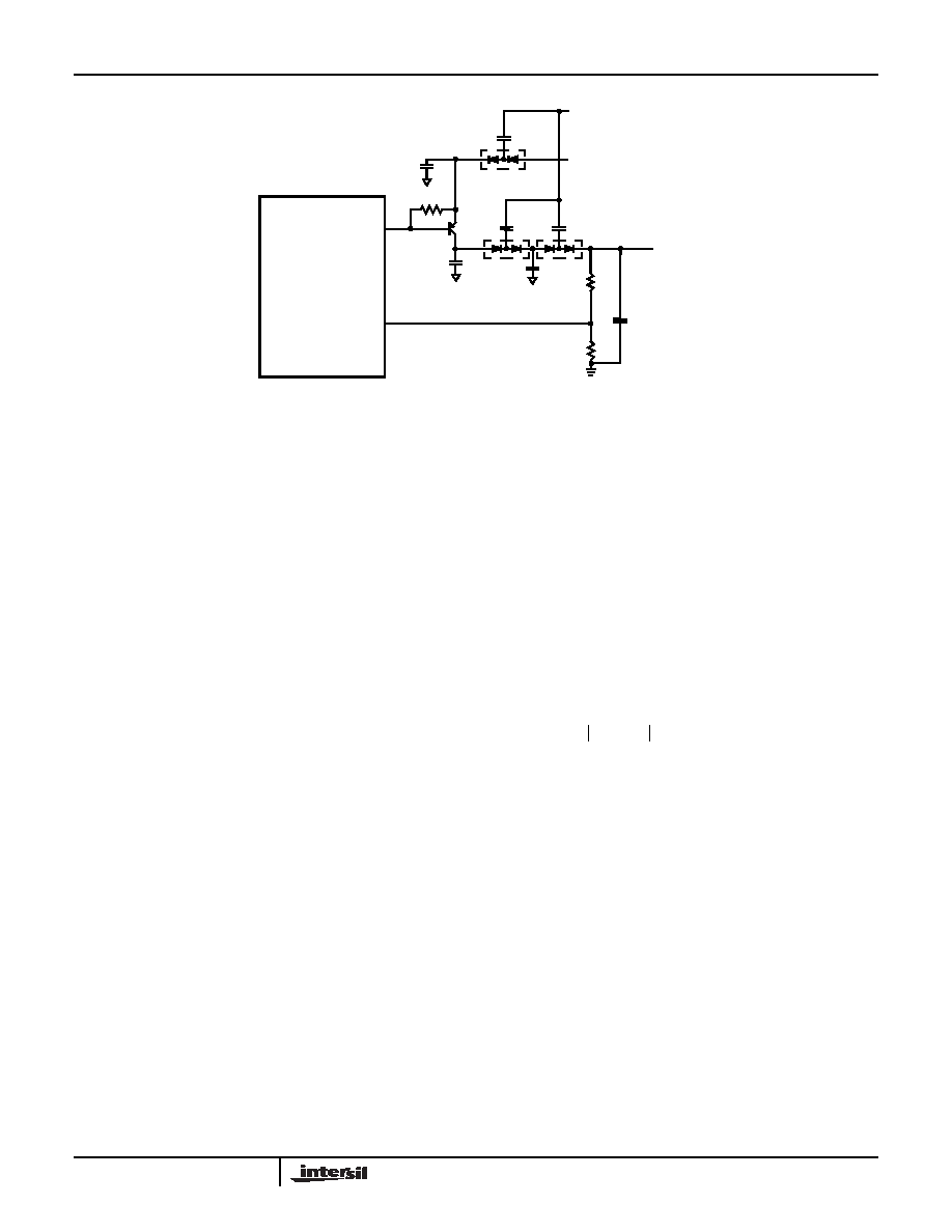
Charge Pump
To generate an output voltage higher than VBOOST, single or
multiple stages of charge pumps are needed. The number of
stage is determined by the input and output voltage. For
positive charge pump stages:
where VCE is the dropout voltage of the pass component of
the linear regulator. It ranges from 0.3V to 1V depending on
the transistor selected. VF is the forward-voltage of the
charge-pump rectifier diode.
The number of negative charge-pump stages is given by:
To achieve high efficiency and low material cost, the lowest
number of charge-pump stages, which can meet the above
requirements, is always preferred.
Charge Pump Output Capacitors
Ceramic capacitor with low ESR is recommended. With
ceramic capacitors, the output ripple voltage is dominated by
the capacitance value. The capacitance value can be
chosen by the following equation:
where fOSC is the switching frequency.
Discontinuous/Continuous Boost Operation and
its Effect on the Charge Pumps
The EL7640A, EL7641A and EL7642A VON and VOFF
architecture uses LX switching edges to drive diode charge
pumps from which LDO regulators generate the VON and
VON
(>36V)
0.1F
0.47F
0.22F
700
0.1F
VBOOST
LX
Q11
FBP
DRVP
EL7642A
FIGURE 22. THE LINEAR REGULATOR CONTROLS ONE STAGE OF CHARGE PUMP
NPOSITIVE
VOUT VCE VINPUT
–
+
VINPUT 2VF
×
–
--------------------------------------------------------------
≥
NNEGATIVE
VOUTPUT VCE
+
VINPUT 2VF
×
–
-------------------------------------------------
≥
COUT
IOUT
2VRIPPLE fOSC
×
------------------------------------------------------
≥
EL7640A, EL7641A, EL7642A
相關PDF資料 |
PDF描述 |
|---|---|
| EL7642AILTZ-T7 | TFT-LCD DC/DC with Integrated Amplifiers |
| EL7900ILCZ-T7 | Ambient Light Photo Detect IC |
| EL8170IS | microPower, Single-Supply, CMOS Instrumentation Amplifier |
| ELEKE222JA | 1 ELEMENT, 2200 uH, GENERAL PURPOSE INDUCTOR |
| ELEKN183KA | 1 ELEMENT, 18000 uH, GENERAL PURPOSE INDUCTOR |
相關代理商/技術參數 |
參數描述 |
|---|---|
| EL7642AILTZ-T7 | 功能描述:LCD 驅動器 EL7642AILTZ TFT-LCD DC-DC W/INTEGRTD AMP RoHS:否 制造商:Maxim Integrated 數位數量:4.5 片段數量:30 最大時鐘頻率:19 KHz 工作電源電壓:3 V to 3.6 V 最大工作溫度:+ 85 C 最小工作溫度:- 20 C 封裝 / 箱體:PDIP-40 封裝:Tube |
| EL7642ILTZ | 功能描述:直流/直流開關調節(jié)器 EL7642ILZ TFT-LCD DC -DC W/INTEGRTD AMP RoHS:否 制造商:International Rectifier 最大輸入電壓:21 V 開關頻率:1.5 MHz 輸出電壓:0.5 V to 0.86 V 輸出電流:4 A 輸出端數量: 最大工作溫度: 安裝風格:SMD/SMT 封裝 / 箱體:PQFN 4 x 5 |
| EL7642ILTZ-T13 | 功能描述:直流/直流開關調節(jié)器 EL7642ILTZ TFT-LCD D C-DC W/INTEGRTD AMP RoHS:否 制造商:International Rectifier 最大輸入電壓:21 V 開關頻率:1.5 MHz 輸出電壓:0.5 V to 0.86 V 輸出電流:4 A 輸出端數量: 最大工作溫度: 安裝風格:SMD/SMT 封裝 / 箱體:PQFN 4 x 5 |
| EL7642ILTZ-T7 | 功能描述:直流/直流開關調節(jié)器 EL7642ILTZ TFT-LCD D C-DC W/INTEGRTD AMP RoHS:否 制造商:International Rectifier 最大輸入電壓:21 V 開關頻率:1.5 MHz 輸出電壓:0.5 V to 0.86 V 輸出電流:4 A 輸出端數量: 最大工作溫度: 安裝風格:SMD/SMT 封裝 / 箱體:PQFN 4 x 5 |
| EL7661CN | 制造商:未知廠家 制造商全稱:未知廠家 功能描述:IC-100V FULL BRIDGE DRIVER |
發(fā)布緊急采購,3分鐘左右您將得到回復。