- 您現(xiàn)在的位置:買賣IC網(wǎng) > PDF目錄362664 > EM19101M (ELAN Microelctronics Corp .) 8-BIT 5 MSPS A/D CONVERTER (CMOS) PDF資料下載
參數(shù)資料
| 型號: | EM19101M |
| 廠商: | ELAN Microelctronics Corp . |
| 英文描述: | 8-BIT 5 MSPS A/D CONVERTER (CMOS) |
| 中文描述: | 8位5 MSPS采樣速率的A / D轉(zhuǎn)換器(CMOS)技術(shù) |
| 文件頁數(shù): | 4/6頁 |
| 文件大小: | 105K |
| 代理商: | EM19101M |
* This specification are subject to be changed without notice.
EM19101
8-BIT 5 MSPS A/D CONVERTER (CMOS)
4
4.23.1997
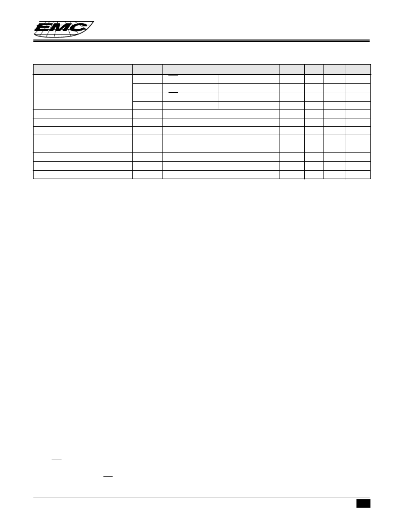
Parameter
Digital output current
Sym.
I
OH
I
OL
I
OZH
Conditions
OE=V
,
V
=min.
OE=V
DD
,
Min. Typ. Max. Unit
-1.1
3.7
V
OH
=V
-0.5V
V
OL
=0.4V
V
OH
=V
DD
V
OL
=0V
mA
Digital output current
16
16
40
1.3
uA
Output data delay
Integral nonlinearity
Differential nonlinearity
Differential gain error
T
EL
ED
DG
25
0.5
±
0.3
±
0.5
ns
F
C
=5MSPS V
IN
=0.6V to 2.6V
F
=5MSPS V
=0.6V to 2.6V
NTSC 40 IRE mod ramp,
F
C
=14.3MSPS
LSB
LSB
1.0
0.5
30
4
%
°
C
ps
ns
Differential phase error
Aperture jitter
Sampling delay
D
P
t
AJ
t
DS
Application Note
V
DD
,V
SS
To reduce noise effects, separate the analog and digital systems close to the device. For both the digital and
analog V
pins, use a ceramic capacitor of about 0.1uF set as close as possible to the pin to bypass to the
respective GND’s.
Analog input
Compared with the flash type A/D converter, the input capacitance of the analog input is rather small. However
it is necessary to conduct the drive with an amplifier featuring sufficient band and drive capability. When
driving with an amplifier of low output impedance, parasite oscillation may occur. That may be prevented by
inserting a resistance of about 100
in series between the amplifier output and A/D input.
Clock input
The clock line wiring should be as short as possible also, to avoid any interference with other signals, separate
it from other circuits
Reference input
Voltage between V
to V
is compatible with the dynamic range of the analog input. Bypassing V
and
V
pins to GND, by means of a capacitor about 0.1
μ
F, stable characteristics are obtained. By shorting V
RT
and V
RTS
, V
RB
and VRBS, the self bias function that generates V
RT
=2.6V and V
RB
=0.6V, is activated.
Timing
Analog input is sampled with the falling edge of external clock and output as digital data with a delay of 2.5
clocks and with the following rising edge. The delay from the clock rising edge to the data output is about 25ns.
OE pin
By connecting OE to GND output mode is obtained. By connecting to V
DD
high impedance is obtained.
相關(guān)PDF資料 |
PDF描述 |
|---|---|
| EM19101S | 8-BIT 5 MSPS A/D CONVERTER (CMOS) |
| EM19110 | 10-BIT 5 MSPS A/D CONVERTER |
| EM19110M | 10-BIT 5 MSPS A/D CONVERTER |
| EM20035 | 3 Seconds Single Chip Voice Synthesizer IC with Built-In On-Chip ROM(帶內(nèi)置片上ROM的語音容量為3秒的單片語音合成器) |
| EM20055A | Single Chip Voice Synthesizer IC(帶內(nèi)置掩膜ROM的單片語音合成IC) |
相關(guān)代理商/技術(shù)參數(shù) |
參數(shù)描述 |
|---|---|
| EM19101S | 制造商:EMC 制造商全稱:ELAN Microelectronics Corp 功能描述:8-BIT 5 MSPS A/D CONVERTER (CMOS) |
| EM19110 | 制造商:EMC 制造商全稱:ELAN Microelectronics Corp 功能描述:10-BIT 5 MSPS A/D CONVERTER |
| EM19110M | 制造商:EMC 制造商全稱:ELAN Microelectronics Corp 功能描述:10-BIT 5 MSPS A/D CONVERTER |
| EM198810 | 制造商:EMC 制造商全稱:ELAN Microelectronics Corp 功能描述:2.4 GHz ISM Band Transceiver/Framer IC |
| EM198810H | 制造商:EMC 制造商全稱:ELAN Microelectronics Corp 功能描述:2.4 GHz ISM Band Transceiver/Framer IC |
發(fā)布緊急采購,3分鐘左右您將得到回復(fù)。