- 您現(xiàn)在的位置:買(mǎi)賣IC網(wǎng) > PDF目錄68993 > FAN5355UC06X (FAIRCHILD SEMICONDUCTOR CORP) 1.8 A SWITCHING CONTROLLER, 3350 kHz SWITCHING FREQ-MAX, PBGA12 PDF資料下載
參數(shù)資料
| 型號(hào): | FAN5355UC06X |
| 廠商: | FAIRCHILD SEMICONDUCTOR CORP |
| 元件分類: | 穩(wěn)壓器 |
| 英文描述: | 1.8 A SWITCHING CONTROLLER, 3350 kHz SWITCHING FREQ-MAX, PBGA12 |
| 封裝: | 2.23 X 1.46 MM, 0.50 MM PITCH, WLCSP-12 |
| 文件頁(yè)數(shù): | 11/26頁(yè) |
| 文件大小: | 1762K |
| 代理商: | FAN5355UC06X |
第1頁(yè)第2頁(yè)第3頁(yè)第4頁(yè)第5頁(yè)第6頁(yè)第7頁(yè)第8頁(yè)第9頁(yè)第10頁(yè)當(dāng)前第11頁(yè)第12頁(yè)第13頁(yè)第14頁(yè)第15頁(yè)第16頁(yè)第17頁(yè)第18頁(yè)第19頁(yè)第20頁(yè)第21頁(yè)第22頁(yè)第23頁(yè)第24頁(yè)第25頁(yè)第26頁(yè)

2008 Fairchild Semiconductor Corporation
19
www.fairchildsemi.com
FAN5355 Rev. 1.0.7
FAN5355
—
1.1A
/
1
A
/
0.8A,
3
M
Hz
Digita
lly
Programmable
Regulator
Switching-Frequency Control and
Synchronization
The nominal internal oscillator frequency is 3MHz. The
regulator runs at its internal clock frequency until these
conditions are met:
1.
EN_SYNC bit, CONTROL1[5], is set; and
2.
A valid frequency appears on the SYNC pin.
CONTROL2
fSYNC Valid
PLL_MULT
fSYNC Divider
Min.
Typ.
Max.
00
1
1.80
3.00
4.00
01
2
0.90
1.50
2.00
10
3
0.60
1.00
1.33
11
4
0.45
0.75
1.00
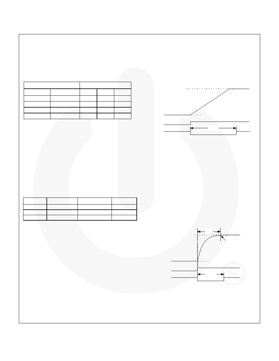
Table 5.SYNC Frequency Validation for fOSC(INTERNAL)=3.0MHz
If the EN_SYNC is set and SYNC fails validation, the regulator
continues to run at its internal oscillator frequency. The
regulator is functional if fSYNC is valid, as defined in Table 5,
but its performance is compromised if fSYNC is outside the fSYNC
window in the Electrical Specifications.
When CONTROL1[3:2] = 00 and the VSEL line is LOW, the
converter
operates
according
to
the
MODE0
bit,
CONTROL1[0], with synchronization disabled regardless of
the state of the EN_SYNC and HW_nSW bits.
Output Voltage Transitions
The IC regulates VOUT to one of two set point voltages, as
determined by the VSEL pin and the HW_nSW bit.
VSEL Pin
HW_nSW Bit
VOUT Set Point
PFM
0
1
VSEL0
Allowed
1
VSEL1
Per MODE1
x
0
VSEL1
Per MODE1
Table 6. VOUT Set Point and Mode Control MODE_CTRL,
CONTROL1[3:2] = 00
If HW_nSW = 0, VOUT transitions are initiated through the
following sequence:
1.
Write the new setpoint in VSEL1.
2.
Write desired transition rate in DEFSLEW,
CONTROL2[2:0], and set the GO bit in CONTROL2[7].
If HW_nSW = 1, VOUT transitions are initiated either by
changing the state of the VSEL pin or by writing to the VSEL
register selected by the VSEL pin.
Positive Transitions
When transitioning to a higher VOUT, the regulator can perform
the transition using multi-step or single-step mode.
Multi-Step Mode:
Applies to Options 03 and 06 only.
The internal DAC is stepped at a rate defined by DEFSLEW,
CONTROL2[2:0], ranging from 000 to 110. This mode
minimizes the current required to charge COUT and thereby
minimizes the current drain from the battery when
transitioning. The PWROK bit, CONTROL2[5], remains LOW
until about 1.5
s after the DAC completes its ramp.
VLOW
VHIGH
VSEL
VOUT
PWROK
t
POK(L-H)
Figure 38. Multi-Step VOUT Transition
Single-Step Mode:
Used if DEFSLEW, CONTROL2[2:0] = 111. The internal DAC
is immediately set to the higher voltage and the regulator
performs the transition as quickly as its current-limit circuit
allows, while avoiding excessive overshoot.
Figure 39 shows single-step transition timing. tV(L-H) is the time
it takes the regulator to settle to within 2% of the new set point
and is typically 7
s for a full-range transition (from 000000 to
111111). The PWROK bit, CONTROL2[5], goes LOW until the
transition is complete and VOUT settled. This typically occurs
~2
s after tV(L-H).
It is good practice to reduce the load current before making
positive VSEL transitions. This reduces the time required to
make positive load transitions and avoids current-limit-induced
overshoot.
t
V(L-H)
VLOW
VHIGH
98% VHIGH
VSEL
VOUT
PWROK
t
POK(L-H)
Figure 39. Single-Step VOUT Transition
All positive VOUT transitions inhibit PFM until the transition is
complete, which occurs at the end of tPOK(L-H).
相關(guān)PDF資料 |
PDF描述 |
|---|---|
| FAN5361UC19X | 0.6 A SWITCHING REGULATOR, 6600 kHz SWITCHING FREQ-MAX, PBGA6 |
| FAN5361UMP182X | 1.25 A SWITCHING REGULATOR, 6600 kHz SWITCHING FREQ-MAX, PDSO6 |
| FAN5361UMP123X | 1.25 A SWITCHING REGULATOR, 6600 kHz SWITCHING FREQ-MAX, PDSO6 |
| FAN5362UC21X | 0.75 A SWITCHING REGULATOR, 3300 kHz SWITCHING FREQ-MAX, PBGA6 |
| FAN5362UMP33X | 1.15 A SWITCHING REGULATOR, 3300 kHz SWITCHING FREQ-MAX, PDSO6 |
相關(guān)代理商/技術(shù)參數(shù) |
參數(shù)描述 |
|---|---|
| FAN5355UC07X | 制造商:FAIRCHILD 制造商全稱:Fairchild Semiconductor 功能描述:1A / 0.8A, 3MHz Digitally Programmable TinyBuckTM Regulator |
| FAN5355UC08X | 功能描述:直流/直流開(kāi)關(guān)轉(zhuǎn)換器 1.1A/1A/0.8A 3MHz Digital PROG REG RoHS:否 制造商:STMicroelectronics 最大輸入電壓:4.5 V 開(kāi)關(guān)頻率:1.5 MHz 輸出電壓:4.6 V 輸出電流:250 mA 輸出端數(shù)量:2 最大工作溫度:+ 85 C 安裝風(fēng)格:SMD/SMT |
| FAN5358 | 制造商:FAIRCHILD 制造商全稱:Fairchild Semiconductor 功能描述:2MHz, 500mA, SC70 Synchronous Buck Regulator |
| FAN5358_10 | 制造商:FAIRCHILD 制造商全稱:Fairchild Semiconductor 功能描述:2MHz, 500mA, SC70 Synchronous Buck Regulator |
| FAN5358S710X | 功能描述:DC/DC 開(kāi)關(guān)控制器 2MHz 500mA Sync. Buck Regulator RoHS:否 制造商:Texas Instruments 輸入電壓:6 V to 100 V 開(kāi)關(guān)頻率: 輸出電壓:1.215 V to 80 V 輸出電流:3.5 A 輸出端數(shù)量:1 最大工作溫度:+ 125 C 安裝風(fēng)格: 封裝 / 箱體:CPAK |
發(fā)布緊急采購(gòu),3分鐘左右您將得到回復(fù)。