- 您現(xiàn)在的位置:買賣IC網(wǎng) > PDF目錄68995 > FSAR001BNY (FAIRCHILD SEMICONDUCTOR CORP) AC-DC REG PWR SUPPLY MODULE PDF資料下載
參數(shù)資料
| 型號: | FSAR001BNY |
| 廠商: | FAIRCHILD SEMICONDUCTOR CORP |
| 元件分類: | 電源模塊 |
| 英文描述: | AC-DC REG PWR SUPPLY MODULE |
| 封裝: | GREEN, MS-001BA, DIP-8 |
| 文件頁數(shù): | 11/12頁 |
| 文件大小: | 494K |
| 代理商: | FSAR001BNY |
2010 Fairchild Semiconductor Corporation
www.fairchildsemi.com
FSAR001 Rev. 1.0.0
8
FSAR001
—
AC-DC
Linear
Regulator
Functional Description
The FSAR001 is a compact, inductor-free, and highly
monolithic AC/DC linear converter housed in 8-lead DIP
packages and designed for non-isolated AC/DC
converter and home appliances. The FSAR001
provides universal AC voltage input from 80VRMS to
265VRMS and fixed-DC output voltage with current limiter
for the non-isolated AC/DC converter operating safety
and stability. The FSAR001 integrates many protection
functions, including output current limiter (ILIMIT), output
under-voltage
protection
(UVP),
over-temperature
protector (OTP), VDD over-voltage protection (OVP), and
AC synchronous signal detect function (VDET).
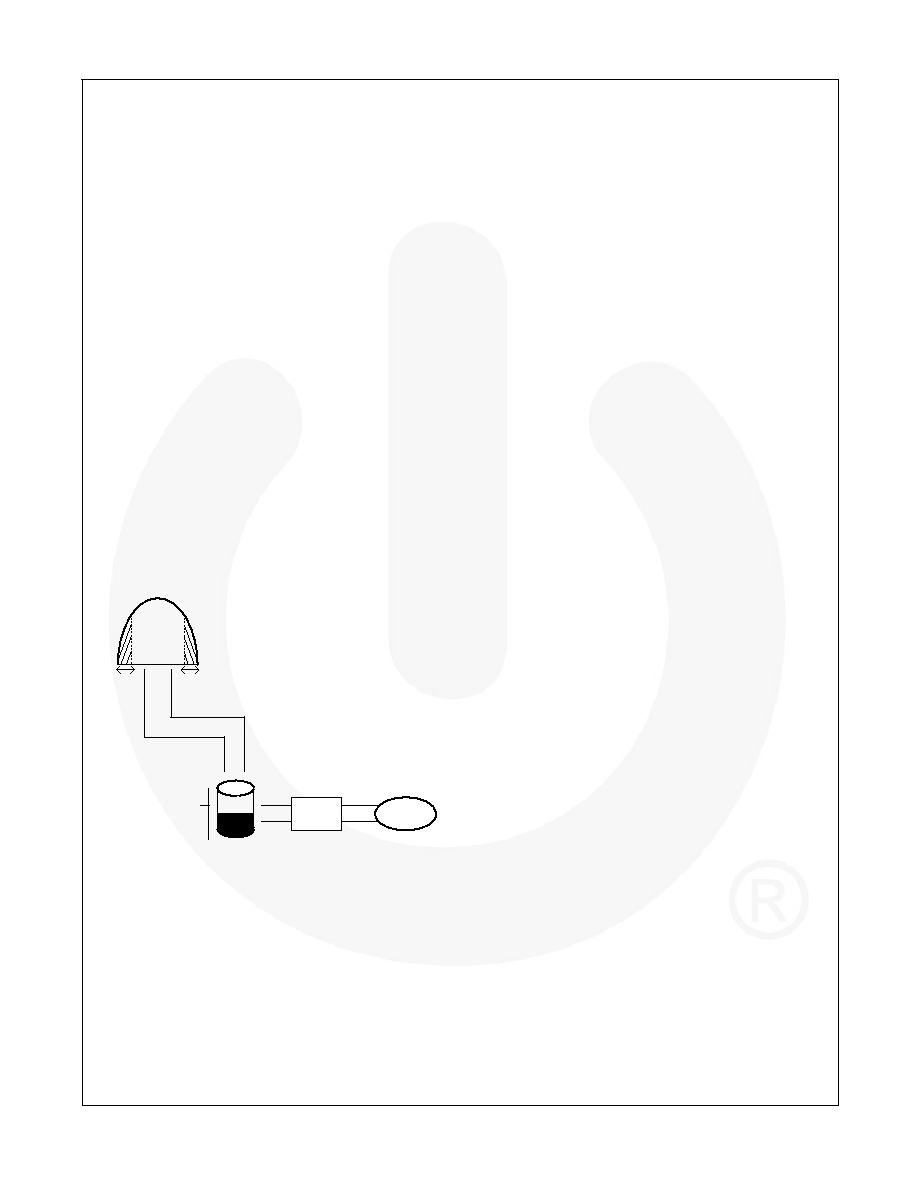
As the FSAR001 operates in a typical application, the
startup current flows through the startup pin (VST) and
charges VDD capacitor. When the voltage of VDD is
larger than VTH_ON, the FSAR001 is turned on. After one
AC synchronous signal, the LDO is turned on and
creates output voltage (VOUT). At steady state, the
energy of VDD capacitor decreases because of the chip
operation and load power dissipation. The behavior is
shown in Figure 17 and the energy is recharged during
conduction angle interval (settled by R3 and R4) and
under OVP function limitation (VDD-OVPH). With a view to
increasing
LDO
efficiency
and
system
stability,
FSAR001 sets the VDD OVP voltage at 8.5V for 5V LDO
regulator. The VDD capacitor recovery angle controls
below 50VRMS settled by AC synchronous signal (DET
sense voltage), detailed in the following sections.
CVDDmax
VIN
Conduction angle
(set by R3&R4)
VDD(capacitance)
IIN
LDO
Load
VOUT
Max
Figure 17. Operating Principle
Startup Current
During FSAR001 startup, the startup current through
the rectifier and VST pin charges the VDD capacitor with
maximum start current of VST pin of 3.75mA and the
synchronous current controlled by R3 (1M) and R4
(13k), shown in Figure 1. The FSAR001 remains off
until the VDD voltage is larger than VTH-ON and the output
voltage is created at the same time. After the FSAR001
turns on, the VST function is disabled by the control
loop. The major energy path changes from VST pin from
the inner power MOSFET MV (VIN).
OUT Pin Under-Voltage Protection
When the output power is larger than the maximum
handling power of FSAR001, the condition causes the
output voltage to drop. Until the output voltage is less
than output nominal voltage -12% (5V – 0.625V =
4.375V), the UVP function disables the LDO stage and
waits until the next AC synchronous signal to restart the
FSAR001 automatically.
Current Limit
The FSAR001 includes a current limiter (ILIMIT) for safe
LDO operation. The limiter monitors the loading current
and directly controls the output delivery current of LDO.
The typical limited current set is 140mA to avoid the
output shorted to ground for an indefinite amount of
time without damaging the part. At over-current
operation, the ILIMIT function limits the maximum output
current and causes the unregulated output voltage to
drop until the UVP function occurs.
Over-Temperature Protection
The FSAR001 operates in highly converting ratio. The
thermal energy of FSAR001 is generated by the inner
converting power of the MOSFET. When the junction
temperature (TJ) exceeds 150°C, the OTP function
disables LDO stage and waits for the next AC
synchronous signal to restart. The over-temperature
hysteresis range is 40°C. After startup, the OTP
function monitors the junction temperature. When
junction temperature decreases to the (TOTP-THYS), the
OTP function enables the signal and allows LDO turn
on. If not, OTP function keeps the output function
disabled and continuously monitors the junction
temperature. The OTP function is designed to protect
against abnormal conditions and over-power operation.
DET Pin Selection
The DET pin connects to the commutated AC bus. It
sinks commutated AC voltage waveform used to
provide the AC synchronous signal and to set the VDD
capacitor recovery conduction angle. For synchronous
signal function, the AC synchronous signal used to
enable output voltage of the LDO and to trigger the
output stage protection with UVP and OTP. To limit the
recovery-conduction angle of the VDD capacitor, the
DET pin sense voltage (VDET) is set between 0.14V
~0.95V. During the sense-voltage range of the DET pin,
the VDD capacitor can be charged by the power
MOSFET until the OVP function is operating in every
synchronous cycle. As shown in Figure 18, the DET pin
sense voltage limits the charge time of t0~t1 and t2~ts/2
settled by R3 and R4. The maximum commutated input
voltage of FSAR001 can be determined by the following
equation with the maximum DET sense voltage defined:
相關(guān)PDF資料 |
PDF描述 |
|---|---|
| FSBH0170NYF116 | 0.9 A SWITCHING CONTROLLER, 106 kHz SWITCHING FREQ-MAX, PDIP8 |
| FSBH0270NYF116 | 1.1 A SWITCHING CONTROLLER, 106 kHz SWITCHING FREQ-MAX, PDIP8 |
| FSBH0370NYF116 | 1.3 A SWITCHING CONTROLLER, 106 kHz SWITCHING FREQ-MAX, PDIP8 |
| FSBH0370NY_F116 | 1.3 A SWITCHING CONTROLLER, 106 kHz SWITCHING FREQ-MAX, DIP8 |
| FSBH0270NY_F116 | 1.1 A SWITCHING CONTROLLER, 106 kHz SWITCHING FREQ-MAX, DIP8 |
相關(guān)代理商/技術(shù)參數(shù) |
參數(shù)描述 |
|---|---|
| FSAR502Y | 制造商:Panduit Corp 功能描述:2 FIBER RISER CABLE, 50UMROUND 制造商:Panduit Corp 功能描述:2 FIBER RISER CABLE, 50UMROUND INTERCONN - Cable Rools/Shrink Tubing |
| FSAR602Y | 制造商:Panduit Corp 功能描述:2 FIBER RISER CABLE, 62.5ROUND 制造商:Panduit Corp 功能描述:2 FIBER RISER CABLE, 62.5ROUND INTERCONN - Cable Rools/Shrink Tubing |
| FSAR902Y | 制造商:Panduit Corp 功能描述:2 FIBER RISER ROUND 2.5MMSM INTERCONNECT - Cable Rools/Shrink Tubing 制造商:Panduit Corp 功能描述:2 FIBER RISER ROUND 2.5MM SM INTERCONNEC |
| FSA-SET | 制造商:Fujitsu Frontech 功能描述:REMOTE SETUP FOR DATABASE APPS - Bulk |
| FSA-SF2-14E2 | 制造商:Amphenol Corporation 功能描述: |
發(fā)布緊急采購,3分鐘左右您將得到回復(fù)。