- 您現(xiàn)在的位置:買賣IC網(wǎng) > PDF目錄67672 > GP2021 (Mitel Networks Corporation) GPS 12 channel Correlator Advance Information PDF資料下載
參數(shù)資料
| 型號(hào): | GP2021 |
| 廠商: | Mitel Networks Corporation |
| 英文描述: | GPS 12 channel Correlator Advance Information |
| 中文描述: | 全球定位系統(tǒng)12通道相關(guān)器研究進(jìn)展信息 |
| 文件頁(yè)數(shù): | 61/62頁(yè) |
| 文件大小: | 372K |
| 代理商: | GP2021 |
第1頁(yè)第2頁(yè)第3頁(yè)第4頁(yè)第5頁(yè)第6頁(yè)第7頁(yè)第8頁(yè)第9頁(yè)第10頁(yè)第11頁(yè)第12頁(yè)第13頁(yè)第14頁(yè)第15頁(yè)第16頁(yè)第17頁(yè)第18頁(yè)第19頁(yè)第20頁(yè)第21頁(yè)第22頁(yè)第23頁(yè)第24頁(yè)第25頁(yè)第26頁(yè)第27頁(yè)第28頁(yè)第29頁(yè)第30頁(yè)第31頁(yè)第32頁(yè)第33頁(yè)第34頁(yè)第35頁(yè)第36頁(yè)第37頁(yè)第38頁(yè)第39頁(yè)第40頁(yè)第41頁(yè)第42頁(yè)第43頁(yè)第44頁(yè)第45頁(yè)第46頁(yè)第47頁(yè)第48頁(yè)第49頁(yè)第50頁(yè)第51頁(yè)第52頁(yè)第53頁(yè)第54頁(yè)第55頁(yè)第56頁(yè)第57頁(yè)第58頁(yè)第59頁(yè)第60頁(yè)當(dāng)前第61頁(yè)第62頁(yè)
8
GP2021
12 CHANNEL CORRELATOR
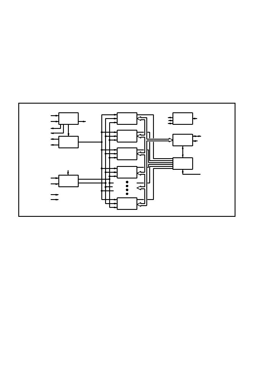
Fig. 4 shows a block diagram of the correlator. It consists
of the following blocks:
Clock Generator
The Clock Generator block divides the frequency of the
master clock CLK_T/CLK_I by 6 or 7 to give the internal multi–
phase set of clocks. When in Real_Input mode CLK_T/CLK_I
will normally be a 40MHz clock, which is divided by 7. When
in Complex_Input mode it will normally be at 35MHz which is
divided by 6. The SAMPCLK pin is an output giving a 4:3
mark–to–space ratio clock at 40 MHz / 7 (= 5714MHz) in
Real_Input Mode.
The Clock Generator also produces the MICRO_CLK
signal at half the master clock frequency (20 MHz for
Real_Input mode, 17.5 MHz for Complex_Input mode) with a
1:1 mark–to–space ratio. This signal is output on the
MICRO_CLK pin in Standard Interface mode. However, its
main purpose is that of a synchronising clock to the memory
control logic in ARM System Mode and it is from this that the
processor clock output, MCLK, is derived.
Timebase Generator
The Timebase Generator produces 4 important timing
signals: ACCUM_INT, TIC, MEAS_INT and TIMEMARK.
ACCUM_INT is an interrupt provided to control data transfer
between the correlator accumulators and the microprocessor.
It may be detected by means of the ACCUM_INT output or by
reading the ACCUM_STATUS_A register (where bit 15 is a
flag indicating that ACCUM_INT has occurred since the
previous read of this register). ACCUM_INT is cleared by
reading ACCUM_STATUS_A.
After power–up this interrupt occurs every 505.05
s. Its
period can subsequently be changed in one of 3 ways:
1) toggling the FRONT_END_MODE bit of the
SYSTEM_SETUP register,
2) toggling the INTERRUPT_PERIOD bit of the
SYSTEM_SETUP register, or
3) writing directly to the PROG_ACCUM_INT register.
See section ‘‘Detailed Description of Registers” on page 25 for
more information.
TIC is an internal signal with a default period of
99999.90
s. It is used to latch measurement data (Epoch
count, Code phase, Code DCO phase, Carrier DCO phase
Fig. 4 Correlator block diagram
and Carrier cycle count) of all 12 channels at the same instant.
Its period can subsequently be changed, by writing to the
PROG_TIC_HIGH and PROG_TIC_LOW registers, or
toggling
the
FRONT_END_MODE
bit
of
the
SYSTEM_SETUP register.
MEAS_INT is a signal derived from the TIC counter. It may
be used by the microprocessor as a software module
switching interrupt either by using the MEAS_INT output or by
reading the ACCUM_STATUS_B or MEAS_STATUS_A
register. MEAS_INT is activated at each TIC and 50 ms before
each TIC so long as the TIC period is greater than 50 ms. If the
TIC period is less than 50 ms, MEAS_INT is activated only at
each
TIC.
It
is
cleared
by
reading
either
the
ACCUM_STATUS_B or MEAS_STATUS_A register,
depending upon the MEAS_INT_SOURCE bit of the
SYSTEM_SETUP register.
TIMEMARK is also derived from TIC and may be output on
one of the discrete output pins. This signal is intended to be
used as an accurate 1 Pulse Per Second timing reference,
aligned to UTC (Universal Time Co–ordinated system), with a
pulse width of 1ms.
TIMEMARK has two methods of operation but in both
TRACKING
MODULE
CHANNEL 0
TRACKING
MODULE
CHANNEL 1
TRACKING
MODULE
CHANNEL 2
TRACKING
MODULE
CHANNEL 3
TRACKING
MODULE
CHANNEL 11
REGISTER
SELECTS
ADDRESS
DECODER
A<9:2>
32 BIT BUS
D<15:0>
CONTROL
BUS
INTERFACE
STATUS
REGISTERS
SYSTEM STATUS
MULTI–
PHASE
CLOCKS
CLOCK
GENERATOR
CLK_T
CLK_I
SAMPCLK
MICRO_CLK
MEAS_INT
ACCUM_INT
TIMEBASE
GENERATOR
TIC
INTERNAL
SAMPCLK
LATCHED
SIGN0 & MAG0
LATCHED
SIGN1 & MAG1
SAMPLE
LATCH
SIGN0 &
MAG0
SIGN1 &
MAG1
V
DD
POWER SUPPLY
V
SS
BITS
相關(guān)PDF資料 |
PDF描述 |
|---|---|
| GRM40Y5V105Z16 | Circular Connector; MIL SPEC:MIL-C-26482, Series I, Solder; Body Material:Aluminum; Series:PT06; No. of Contacts:21; Connector Shell Size:22; Connecting Termination:Solder; Circular Shell Style:Straight Plug; Body Style:Straight |
| GRM42-6X5R475K10 | 50/100M SOT-23 CMOS RF LDO REGULATORS |
| GT- 32090 | Highly Integrated Single-Chip System Controller(高集成單片系統(tǒng)控制器) |
| GT-48001A | Switched Ethernet Controller For 10BaseX(10BaseX交換式快速以太網(wǎng)控制器) |
| GT-48002A | Switched Fast Ethernet Controller for 100BaseX(100BaseX交換式快速以太網(wǎng)控制器) |
相關(guān)代理商/技術(shù)參數(shù) |
參數(shù)描述 |
|---|---|
| GP2021IGGQ1R | 制造商:未知廠家 制造商全稱:未知廠家 功能描述:Correlator |
| GP202K | 制造商:GTM 制造商全稱:GTM 功能描述:SURFACE MOUNT,SWITCHING DIODE |
| GP2030S | 制造商:GTM 制造商全稱:GTM 功能描述:N AND P-CHANNEL ENHANCEMENT MODE POWER MOSFET |
| GP2-031X250-50 | 制造商:GROOV-PIN 功能描述: |
| GP204 | 制造商:DEC 制造商全稱:DEC 功能描述:2 AMP SOFT GLASS PASSIVATED DIODES |
發(fā)布緊急采購(gòu),3分鐘左右您將得到回復(fù)。