- 您現(xiàn)在的位置:買賣IC網(wǎng) > PDF目錄299161 > GS8662S36BGD-300 (GSI TECHNOLOGY) 2M X 36 STANDARD SRAM, 0.45 ns, PBGA165 PDF資料下載
參數(shù)資料
| 型號: | GS8662S36BGD-300 |
| 廠商: | GSI TECHNOLOGY |
| 元件分類: | SRAM |
| 英文描述: | 2M X 36 STANDARD SRAM, 0.45 ns, PBGA165 |
| 封裝: | 13 X 15 MM, 1 MM PITCH, ROHS COMPLIANT, MO-216CAB-1, FPBGA-165 |
| 文件頁數(shù): | 4/37頁 |
| 文件大?。?/td> | 748K |
| 代理商: | GS8662S36BGD-300 |
第1頁第2頁第3頁當(dāng)前第4頁第5頁第6頁第7頁第8頁第9頁第10頁第11頁第12頁第13頁第14頁第15頁第16頁第17頁第18頁第19頁第20頁第21頁第22頁第23頁第24頁第25頁第26頁第27頁第28頁第29頁第30頁第31頁第32頁第33頁第34頁第35頁第36頁第37頁
GS8662S08/09/18/36BD-400/350/333/300/250
Specifications cited are subject to change without notice. For latest documentation see http://www.gsitechnology.com.
Rev: 1.02 3/2011
12/37
2011, GSI Technology
FLXDrive-II Output Driver Impedance Control
HSTL I/O SigmaSIO DDR-II SRAMs are supplied with programmable impedance output drivers. The ZQ pin must be connected
to VSS via an external resistor, RQ, to allow the SRAM to monitor and adjust its output driver impedance. The value of RQ must be
5X the value of the intended line impedance driven by the SRAM. The allowable range of RQ to guarantee impedance matching
with a vendor-specified tolerance is between 175
Ω and 350Ω. Periodic readjustment of the output driver impedance is necessary as
the impedance is affected by drifts in supply voltage and temperature. The SRAM’s output impedance circuitry compensates for
drifts in supply voltage and temperature every 1024 cycles. A clock cycle counter periodically triggers an impedance evaluation,
resets and counts again. Each impedance evaluation may move the output driver impedance level one step at a time towards the
optimum level.
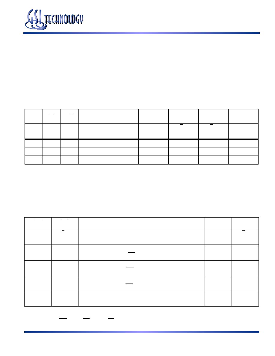
Separate I/O Burst of 2 Sigma SIO-II SRAM Truth Table
A
LD
R/W
Current
Operation
D
Q
K
↑
(tn)
K
↑
(tn)
K
↑
(tn)
K
↑
(tn)
K
↑
(tn + 1)
K
↑
(tn + 1)
K
↑
(tn + 1)
K
↑
(tn + 2)
X
1
X
Deselect
X
Hi-Z
V
0
1
Read
X
Q0
Q1
V
0
Write
D0
D1
Hi-Z
Notes:
1. “1” = input “high”; “0” = input “l(fā)ow”; “V” = input “valid”; “X” = input “don’t care”
2. Q0 and Q1 indicate the first and second pieces of output data transferred during Read operations.
3. D0 and D1 indicate the first and second pieces of input data transferred during Write operations.
4. Users should not clock in metastable addresses.
Burst of 2 Byte Write Clock Truth Table
BW
Current Operation
D
K
↑
(tn + 1)
K
↑
(tn + 1)
K
↑
(tn)
K
↑
(tn + 1)
K
↑
(tn + 1)
T
Write
Dx stored if BWn = 0 in both data transfers
D1
D2
T
F
Write
Dx stored if BWn = 0 in 1st data transfer only
D1
X
F
T
Write
Dx stored if BWn = 0 in 2nd data transfer only
X
D2
F
Write Abort
No Dx stored in either data transfer
X
Notes:
1. “1” = input “high”; “0” = input “l(fā)ow”; “X” = input “don’t care”; “T” = input “true”; “F” = input “false”.
2. If one or more BWn = 0, then BW = “T”, else BW = “F”.
相關(guān)PDF資料 |
PDF描述 |
|---|---|
| GS88036T-100T | 256K X 36 CACHE SRAM, 12 ns, PQFP100 |
| GS88037CT-250I | 256K X 36 CACHE SRAM, 2.3 ns, PQFP100 |
| GS880E18GT-66I | 512K X 18 CACHE SRAM, 18 ns, PQFP100 |
| GS880F18T-14T | 512K X 18 CACHE SRAM, 14 ns, PQFP100 |
| GS880Z18AGT-133I | 512K X 18 ZBT SRAM, 8.5 ns, PQFP100 |
相關(guān)代理商/技術(shù)參數(shù) |
參數(shù)描述 |
|---|---|
| GS8662S36E-167 | 制造商:GSI 制造商全稱:GSI Technology 功能描述:72Mb Burst of 2 DDR SigmaSIO-II SRAM |
| GS8662S36E-167I | 制造商:GSI 制造商全稱:GSI Technology 功能描述:72Mb Burst of 2 DDR SigmaSIO-II SRAM |
| GS8662S36E-200 | 制造商:GSI 制造商全稱:GSI Technology 功能描述:72Mb Burst of 2 DDR SigmaSIO-II SRAM |
| GS8662S36E-200I | 制造商:GSI 制造商全稱:GSI Technology 功能描述:72Mb Burst of 2 DDR SigmaSIO-II SRAM |
| GS8662S36E-250 | 制造商:GSI 制造商全稱:GSI Technology 功能描述:72Mb Burst of 2 DDR SigmaSIO-II SRAM |
發(fā)布緊急采購,3分鐘左右您將得到回復(fù)。