- 您現(xiàn)在的位置:買賣IC網(wǎng) > PDF目錄384398 > HE84760B (King Billion Electronics Co., Ltd.) 8-bit Micro-controller PDF資料下載
參數(shù)資料
| 型號(hào): | HE84760B |
| 廠商: | King Billion Electronics Co., Ltd. |
| 英文描述: | 8-bit Micro-controller |
| 中文描述: | 8位微控制器 |
| 文件頁(yè)數(shù): | 13/51頁(yè) |
| 文件大小: | 487K |
| 代理商: | HE84760B |
第1頁(yè)第2頁(yè)第3頁(yè)第4頁(yè)第5頁(yè)第6頁(yè)第7頁(yè)第8頁(yè)第9頁(yè)第10頁(yè)第11頁(yè)第12頁(yè)當(dāng)前第13頁(yè)第14頁(yè)第15頁(yè)第16頁(yè)第17頁(yè)第18頁(yè)第19頁(yè)第20頁(yè)第21頁(yè)第22頁(yè)第23頁(yè)第24頁(yè)第25頁(yè)第26頁(yè)第27頁(yè)第28頁(yè)第29頁(yè)第30頁(yè)第31頁(yè)第32頁(yè)第33頁(yè)第34頁(yè)第35頁(yè)第36頁(yè)第37頁(yè)第38頁(yè)第39頁(yè)第40頁(yè)第41頁(yè)第42頁(yè)第43頁(yè)第44頁(yè)第45頁(yè)第46頁(yè)第47頁(yè)第48頁(yè)第49頁(yè)第50頁(yè)第51頁(yè)
8.
LCD Display RAM Map
KING BILLION ELECTRONICS CO., LTD
駿
億
電
子
股
份
有
限
公
司
HE84760B
HE80004 Series
June 29, 2005
This specification is subject to change without notice. Please contact sales person for the latest version before use.
13
V1.0
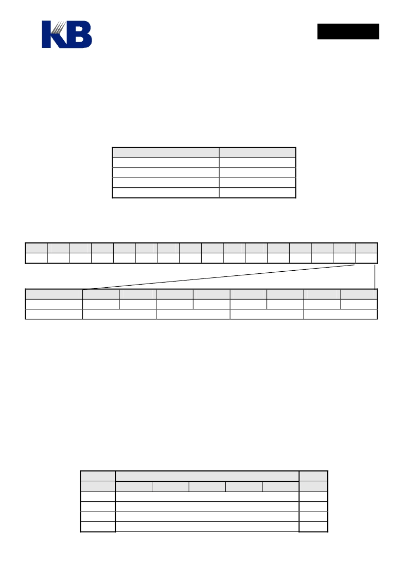
The gray-scale LCD driver can be configured to be a 4 gray-scales or black and white display by mask
option MO_GRAY_MODE.
MO_GRAY_MODE[1..0]
00
01
10
11
Gray levels
Not allowed
4
2 (B/W)
2 (B/W)
For 4 gray-scale display, 2-bit of RAM is required for each pixel and 1-bit for black and white display.
For different LCD configuration, the LCD display RAM is arranged differently. The following figure
shows one byte of RAM in different LCD configurations:
0F
xx
0E
xx
0D
xx
0C
xx
0B
xx
0A
xx
09
xx
08
xx
07
xx
06
xx
05
xx
04
xx
03
xx
02
xx
01
xx
00
xx
Black/White
4 Gray scales
Bit 7
SEG7
Bit 6
SEG6
Bit 5
SEG5
Bit 4
SEG4
Bit 3
SEG3
Bit 2
SEG2
Bit 1
SEG1
Bit 0
SEG0
SEG3
SEG2
SEG1
SEG0
The 4 Gray Scale register GRAY0 ~ GRAY3 is the mapping register between the levels selected in RAM
and the real gray scale. In other words, if the content of GRAY0 is 0x03, when value of a certain pixel is
0, the displayed effect will correspond to actual gray level 3. The 4 gray scale display utilizes registers
GRAY0 ~ GRAY3 to select among 32 gray levels to correspond to level 0 ~ 3. Thus user can pick the
gray levels which give the best and most linear effect.
4 Gray Scale registers share a common register address GRAY16. When writing is made to the register, it
will step down to next register in order. The writing sequence can be reset by clearing bit 5 of LCDC
register.
GRAY16
Seq.
1
2
3
4
Field
Bit2
GRAY0
GRAY1
GRAY2
GRAY3
Bit4
Bit3
Bit1
Bit0
Reset
0x00
0x02
0x04
0x06
相關(guān)PDF資料 |
PDF描述 |
|---|---|
| HE84760 | 8-bit Micro-controller |
| HE84761 | 8-bit Micro-controller |
| HE847701 | 8-bit Micro-controller |
| HE84770D | 8-bit Micro-controller |
| HE84770 | 8-bit Micro-controller |
相關(guān)代理商/技術(shù)參數(shù) |
參數(shù)描述 |
|---|---|
| HE84761 | 制造商:KB 制造商全稱:KB 功能描述:8-bit Micro-controller |
| HE84761(S) | 制造商:未知廠家 制造商全稱:未知廠家 功能描述: |
| HE84762(S) | 制造商:未知廠家 制造商全稱:未知廠家 功能描述: |
| HE84770 | 制造商:KB 制造商全稱:KB 功能描述:8-bit Micro-controller |
| HE84770(S) | 制造商:未知廠家 制造商全稱:未知廠家 功能描述: |
發(fā)布緊急采購(gòu),3分鐘左右您將得到回復(fù)。