- 您現(xiàn)在的位置:買賣IC網(wǎng) > PDF目錄384398 > HE84760B (King Billion Electronics Co., Ltd.) 8-bit Micro-controller PDF資料下載
參數(shù)資料
| 型號(hào): | HE84760B |
| 廠商: | King Billion Electronics Co., Ltd. |
| 英文描述: | 8-bit Micro-controller |
| 中文描述: | 8位微控制器 |
| 文件頁數(shù): | 4/51頁 |
| 文件大小: | 487K |
| 代理商: | HE84760B |
第1頁第2頁第3頁當(dāng)前第4頁第5頁第6頁第7頁第8頁第9頁第10頁第11頁第12頁第13頁第14頁第15頁第16頁第17頁第18頁第19頁第20頁第21頁第22頁第23頁第24頁第25頁第26頁第27頁第28頁第29頁第30頁第31頁第32頁第33頁第34頁第35頁第36頁第37頁第38頁第39頁第40頁第41頁第42頁第43頁第44頁第45頁第46頁第47頁第48頁第49頁第50頁第51頁
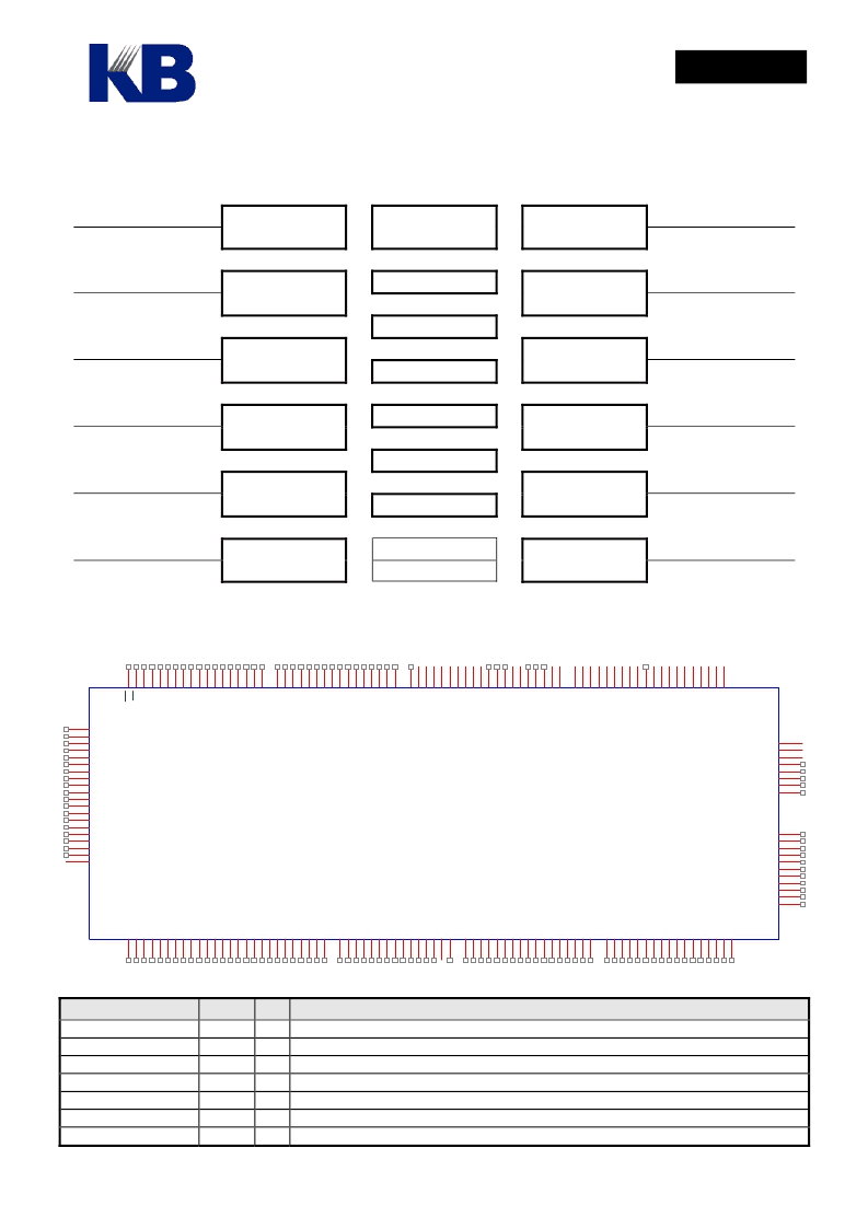
3.
Functional Block Diagram
KING BILLION ELECTRONICS CO., LTD
駿
億
電
子
股
份
有
限
公
司
HE84760B
HE80004 Series
June 29, 2005
This specification is subject to change without notice. Please contact sales person for the latest version before use.
4
V1.0
SEG
COM
FXI, FXO
LCD
Driver
LCD Power
Supply
Segment Ext.
Interface
Ext. Memory
Interface
8 Bit CPU
Fast Clock
OSC.
Slow Clock
OSC
LVL[5..1], LGS1,LVREG
LCAPA, LCAPB
512 KB ROM
SXI, SXO
5 KB RAM
TC1
TC2
TBI
WDT
LVR
LVD
OLFR, OCCK
PWM
PWM
SEGA, SEGD
VO, DAO
DAC
PRTC, PRTD, PRT10,
OPO,OPIN, OPIP
PRT17
I/O Port
OP Amp
SIN, SOUT
IRO
UART
IR
4.
Pin Description
HE84G763B
U1
3
4
5
6
7
8
9
10
11
12
13
14
15
16
17
18
19
20
2
2
2
2
2
2
2
2
2
3
3
3
3
3
3
3
3
4
4
4
4
4
4
4
4
4
4
5
5
5
5
5
5
5
6
6
6
6
6
6
6
6
7
7
7
7
7
7
7
7
7
7
8
8
8
9
8
8
8
8
8
8
9
9
9
96
97
98
99
100
107
108
109
110
111
1
1
1
1
1
1
1
1
1
1
1
1
1
1
1
1
1
1
1
1
1
1
1
1
1
1
1
1
1
1
1
1
1
1
2
1
1
3
3
5
5
5
6
6
8
9
9
112
113
114
1
1
1
1
1
1
1
1
1
1
1
1
1
1
1
1
1
1
1
1
1
1
1
1
1
1
1
1
1
1
1
1
1
1
1
1
1
1
1
SEG11/CS2
SEG10/CS3
PRT15[1]
PRT15[0]
PRT17[7]
PRT17[6]
COM25
C
C
C
C
C
C
C
C
C
C
C
C
C
C
C
C
C
C
C
C
C
C
C
C
L
L
L
L
L
L
L
L
L
L
V
O
O
G
O
O
O
D
V
R
F
F
T
S
S
V
V
P
P
P
P
P
P
P
P
P
P
P
P
P
P
PRTC[6]
PRTC[5]
PRTC[4]
PRTC[2]
VDPRTIRO
GND_PWM
CMSG32
CMSG35
CMSG36
CMSG37
CMSG38
CMSG39
C
C
S
S
S
S
S
S
S
S
S
S
S
S
S
S
S
S
S
S
S
S
S
S
S
S
S
S
S
S
S
S
S
S
S
S
SEG12/CS1
C
SEG13/CS0
C
C
L
L
L
L
V
P
P
P
C
C
C
C
C
C
C
C
C
C
C
C
C
C
C
C
C
C
C
C
C
C
C
C
C
C
C
C
C
C
C
C
C
C
C
C
C
Pin Name
COM[31..0]
LVL1
LVL2
LVL3
LVL4
LVL5
LCAP4A
Pin # I/O
15 ~ 46
47
48
49
50
51
52
Description
O LCD COMMON Driver pads.
P LCD Bias Voltage 1.
P LCD Bias Voltage 2
P LCD Bias Voltage 3
P LCD Bias Voltage 4
P LCD Bias Voltage 5.
O Charge Pump Capacitor Pin
相關(guān)PDF資料 |
PDF描述 |
|---|---|
| HE84760 | 8-bit Micro-controller |
| HE84761 | 8-bit Micro-controller |
| HE847701 | 8-bit Micro-controller |
| HE84770D | 8-bit Micro-controller |
| HE84770 | 8-bit Micro-controller |
相關(guān)代理商/技術(shù)參數(shù) |
參數(shù)描述 |
|---|---|
| HE84761 | 制造商:KB 制造商全稱:KB 功能描述:8-bit Micro-controller |
| HE84761(S) | 制造商:未知廠家 制造商全稱:未知廠家 功能描述: |
| HE84762(S) | 制造商:未知廠家 制造商全稱:未知廠家 功能描述: |
| HE84770 | 制造商:KB 制造商全稱:KB 功能描述:8-bit Micro-controller |
| HE84770(S) | 制造商:未知廠家 制造商全稱:未知廠家 功能描述: |
發(fā)布緊急采購,3分鐘左右您將得到回復(fù)。