- 您現(xiàn)在的位置:買賣IC網(wǎng) > PDF目錄371822 > HIP6521EVAL1 (Intersil Corporation) PWM and Triple Linear Power Controller PDF資料下載
參數(shù)資料
| 型號: | HIP6521EVAL1 |
| 廠商: | Intersil Corporation |
| 元件分類: | 基準(zhǔn)電壓源/電流源 |
| 英文描述: | PWM and Triple Linear Power Controller |
| 中文描述: | PWM和三線性功率控制器 |
| 文件頁數(shù): | 4/13頁 |
| 文件大小: | 154K |
| 代理商: | HIP6521EVAL1 |
4
Absolute Maximum Ratings
Thermal Information
UGATE, BOOT. . . . . . . . . . . . . . . . . . . . . . . . . . .GND - 0.3V to 15V
VCC, PHASE . . . . . . . . . . . . . . . . . . . . . . . . . . . .GND - 0.3V to +7V
DRIVE, LGATE, all other pins . . . . . . . . GND - 0.3V to VCC + 0.3V
ESD Classification . . . . . . . . . . . . . . . . . . . . . . . . . . . . . . . . . . . TBD
Operating Conditions
Supply Voltage on VCC . . . . . . . . . . . . . . . . . . . . . . . . . . +5V
±
10%
Ambient Temperature Range. . . . . . . . . . . . . . . . . . . . 0
o
C to 70
o
C
Junction Temperature Range. . . . . . . . . . . . . . . . . . . 0
o
C to 125
o
C
Thermal Resistance (Typical, Note 1)
SOIC Package. . . . . . . . . . . . . . . . . . . . . . . . . . . . .
Maximum Junction Temperature (Plastic Package) . . . . . . . 150
o
C
Maximum Storage Temperature Range. . . . . . . . . . -65
o
C to 150
o
C
Maximum Lead Temperature (Soldering 10s) . . . . . . . . . . . . 300
o
C
(SOIC - Lead Tips Only)
θ
JA
(
o
C/W)
110
CAUTION: Stresses above those listed in “Absolute Maximum Ratings” may cause permanent damage to the device. This is a stress only rating and operation of the
device at these or any other conditions above those indicated in the operational sections of this specification is not implied.
NOTE:
1.
θ
JA
is measured with the component mounted on a low effective thermal conductivity test board in free air. See Tech Brief TB379 for details.
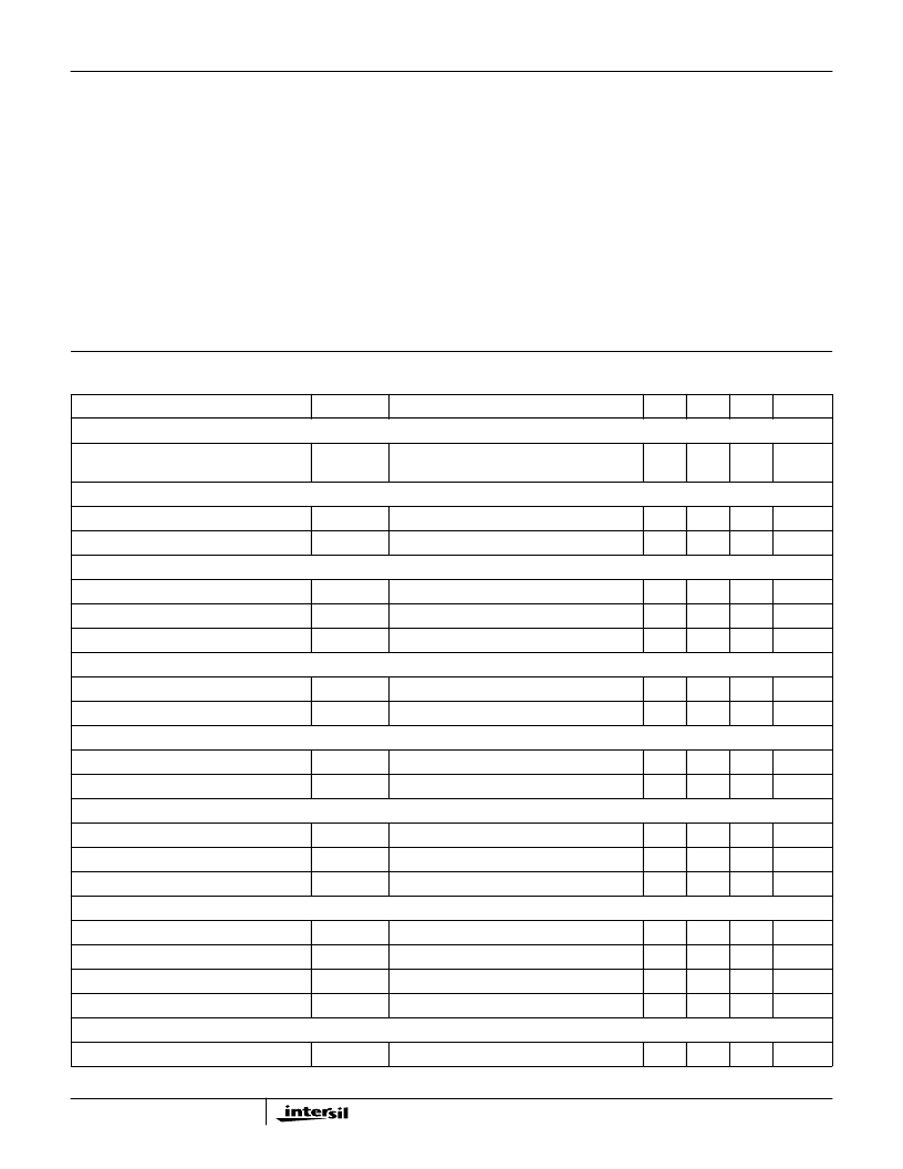
Electrical Specifications
Recommended Operating Conditions, Unless Otherwise Noted. Refer to Block and Simplified Power System
Diagrams, and Typical Application Schematic
PARAMETER
SYMBOL
TEST CONDITIONS
MIN
TYP
MAX
UNITS
VCC SUPPLY CURRENT
Nominal Supply Current
I
CC
UGATE, LGATE, DRIVE2, DRIVE3, and
DRIVE4 Open
-
5
-
mA
POWER-ON RESET
Rising VCC Threshold
4.25
-
4.5
V
Falling VCC Threshold
3.75
-
4.0
V
OSCILLATOR AND SOFT-START
Free Running Frequency
F
OSC
275
300
325
kHz
Ramp Amplitude
V
OSC
-
1.5
-
V
P-P
Soft-Start Interval
T
SS
6.25
6.83
7.40
ms
REFERENCE VOLTAGE
Reference Voltage (All Regulators)
V
REF
-
0.800
-
V
All Outputs Voltage Regulation
-2.0
-
+2.0
%
LINEAR REGULATORS (OUT2, OUT3, AND OUT4)
Output Drive Current (All Linears)
VCC > 4.5V
100
120
-
mA
Undervoltage Level (V
FB
/V
REF
)
V
UV
-
70
-
%
SYNCHRONOUS PWM CONTROLLER ERROR AMPLIFIER
DC Gain
-
80
-
dB
Gain-Bandwidth Product
GBWP
15
-
-
MHz
Slew Rate
SR
COMP = 10pF
-
6
-
V/
μ
s
PWM CONTROLLER GATE DRIVERS
UGATE Source
I
UGATE
VCC = 5V, V
UGATE
= 2.5V
-
-1
-
A
UGATE Sink
I
UGATE
V
UGATE-PHASE
= 2.5V
-
1
-
A
LGATE Source
I
LGATE
VCC = 5V, V
LGATE
= 2.5V
-
-1
-
A
LGATE Sink
I
LGATE
V
LGATE
= 2.5V
-
2
-
A
PROTECTION
OCSET Current Source
I
OCSET
34
40
46
μ
A
HIP6521
相關(guān)PDF資料 |
PDF描述 |
|---|---|
| HIP6602BCRZ-T | Dual Channel Synchronous Rectified Buck MOSFET Driver |
| HIP6602BCRZA | Dual Channel Synchronous Rectified Buck MOSFET Driver |
| HIP6602BCRZA-T | Dual Channel Synchronous Rectified Buck MOSFET Driver |
| HIP6602B | Dual Channel Synchronous Rectified Buck MOSFET Driver |
| HIP6602BCBZ-T | Dual Channel Synchronous Rectified Buck MOSFET Driver |
相關(guān)代理商/技術(shù)參數(shù) |
參數(shù)描述 |
|---|---|
| HIP6601 | 制造商:INTERSIL 制造商全稱:Intersil Corporation 功能描述:Synchronous-Rectified Buck MOSFET Drivers |
| HIP6601_04 | 制造商:INTERSIL 制造商全稱:Intersil Corporation 功能描述:Synchronous-Rectified Buck MOSFET Drivers |
| HIP6601A | 制造商:INTERSIL 制造商全稱:Intersil Corporation 功能描述:Synchronous Rectified Buck MOSFET Drivers |
| HIP6601ACB | 制造商:INTERSIL 制造商全稱:Intersil Corporation 功能描述:Synchronous Rectified Buck MOSFET Drivers |
| HIP6601ACB-T | 制造商:Rochester Electronics LLC 功能描述:- Bulk |
發(fā)布緊急采購,3分鐘左右您將得到回復(fù)。