- 您現(xiàn)在的位置:買賣IC網(wǎng) > PDF目錄371822 > HIP6521EVAL1 (Intersil Corporation) PWM and Triple Linear Power Controller PDF資料下載
參數(shù)資料
| 型號(hào): | HIP6521EVAL1 |
| 廠商: | Intersil Corporation |
| 元件分類: | 基準(zhǔn)電壓源/電流源 |
| 英文描述: | PWM and Triple Linear Power Controller |
| 中文描述: | PWM和三線性功率控制器 |
| 文件頁數(shù): | 6/13頁 |
| 文件大小: | 154K |
| 代理商: | HIP6521EVAL1 |
6
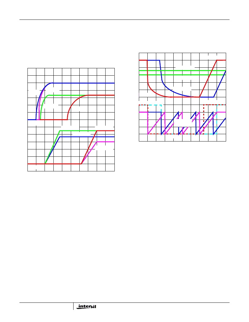
output voltage. As the internal soft-start voltage increases, the
pulse-width on the PHASE pin increases to reach its steady-
state duty cycle at time T2. At time T3, the 3.3V input supply
starts ramping up; as a result, V
OUT2
and V
OUT4
start ramping
up on the second attempt (approximately 3.25 SS cycles wait),
at time T4. During the interval between T4 and T5, the linear
controller error amplifiers’ references ramp to the final value
bringing all outputs within regulation limits.
Overcurrent Protection
All outputs are protected against excessive overcurrents.
The PWM controller uses the upper MOSFET’s
on-resistance, r
DS(ON)
to monitor the current for protection
against shorted output. All linear controllers monitor their
respective FB pins for undervoltage events to protect against
excessive currents.
A sustained overload (undervoltage on linears or overcurrent
on the PWM) on any output results in an independent
shutdown of the respective output, followed by subsequent
individual re-start attempts performed at an interval equivalent
to 3 soft-start intervals. Figure 2 describes the protection
feature. At time T0, an overcurrent event sensed across the
switching regulator’s upper MOSFET (r
DS(ON)
sensing)
triggers a shutdown of the V
OUT1
output. As a result, its
internal soft-start initiates a number of soft-start cycles. After a
three-cycle wait, the fourth soft-start initiates a ramp-up
attempt of the failed output, at time T2, bringing the output in
regulation at time T4.
To exemplify an UV event on one of the linears, at time T1,
the clock regulator (V
OUT2
) is also subjected to an
overcurrent event, resulting in an UV condition. Similarly,
after three soft-start periods, the fourth cycle initiates a
ramp-up of this linear output at time T3. One soft-start period
after T3, the linear output is within regulation limits. UV
glitches less than 1
μ
s (typically) in duration are ignored.
As overcurrent protection is performed on the synchronous
switcher regulator on a cycle-by-cycle basis, OC monitoring
is active as long as the regulator is operational. Since the
overcurrent protection on the linear regulators is performed
through undervoltage monitoring at the feedback pins (FB2,
FB3, and FB4), this feature is activated approximately 25%
into the soft-start interval (see Figure 2).
A resistor (R
OCSET
) programs the overcurrent trip level for
the PWM converter. As shown in Figure 3, the internal
40
μ
A current sink (I
OCSET
) develops a voltage across
R
OCSET
(V
SET
) that is referenced to V
IN
. The DRIVE
signal enables the overcurrent comparator (OCC). When
the voltage across the upper MOSFET (V
DS(ON)
) exceeds
V
SET
, the overcurrent comparator trips to set the
overcurrent latch. Both V
SET
and V
DS(ON)
are referenced
to V
IN
and a small capacitor across R
OCSET
helps V
OCSET
track the variations of V
IN
due to MOSFET switching. The
overcurrent function will trip at a peak inductor current
(I
PEAK)
determined by:
×
DS ON
)
The OC trip point varies with MOSFET’s r
DS(ON)
temperature variations. To avoid overcurrent tripping in the
normal operating load range, determine the R
OCSET
resistor from the equation above with:
FIGURE 1. SOFT-START INTERVAL
0V
0V
TIME
+5V
SB
(0.5V/DIV)
V
OUT2
(2.5V)
V
OUT4
(1.5V)
T1
T2
T3
T0
T4
(1V/DIV)
+3.3V
IN
+5V
DUAL
+3.3V
DUAL
V
OUT3
(1.8V)
V
OUT1
(2.5V)
T5
FIGURE2. OVERCURRENT/UNDERVOLTAGEPROTECTION
RESPONSE
0V
TIME
(0.5V/DIV.)
V
OUT3
(1.8V)
V
OUT2
(2.5V)
T1
T2
T3
T0
V
OUT4
(1.5V)
V
OUT1
(2.5V)
UV MONITORING
INACTIVE
SOFT-START
FUNCTION
ACTIVE
T4
I
PEAK
=
I
-------------r
R
OCSET
HIP6521
相關(guān)PDF資料 |
PDF描述 |
|---|---|
| HIP6602BCRZ-T | Dual Channel Synchronous Rectified Buck MOSFET Driver |
| HIP6602BCRZA | Dual Channel Synchronous Rectified Buck MOSFET Driver |
| HIP6602BCRZA-T | Dual Channel Synchronous Rectified Buck MOSFET Driver |
| HIP6602B | Dual Channel Synchronous Rectified Buck MOSFET Driver |
| HIP6602BCBZ-T | Dual Channel Synchronous Rectified Buck MOSFET Driver |
相關(guān)代理商/技術(shù)參數(shù) |
參數(shù)描述 |
|---|---|
| HIP6601 | 制造商:INTERSIL 制造商全稱:Intersil Corporation 功能描述:Synchronous-Rectified Buck MOSFET Drivers |
| HIP6601_04 | 制造商:INTERSIL 制造商全稱:Intersil Corporation 功能描述:Synchronous-Rectified Buck MOSFET Drivers |
| HIP6601A | 制造商:INTERSIL 制造商全稱:Intersil Corporation 功能描述:Synchronous Rectified Buck MOSFET Drivers |
| HIP6601ACB | 制造商:INTERSIL 制造商全稱:Intersil Corporation 功能描述:Synchronous Rectified Buck MOSFET Drivers |
| HIP6601ACB-T | 制造商:Rochester Electronics LLC 功能描述:- Bulk |
發(fā)布緊急采購,3分鐘左右您將得到回復(fù)。