- 您現在的位置:買賣IC網 > PDF目錄371881 > HPC26003 (National Semiconductor Corporation) High-Performance microControllers PDF資料下載
參數資料
| 型號: | HPC26003 |
| 廠商: | National Semiconductor Corporation |
| 英文描述: | High-Performance microControllers |
| 中文描述: | 高性能微控制器 |
| 文件頁數: | 12/36頁 |
| 文件大?。?/td> | 467K |
| 代理商: | HPC26003 |
第1頁第2頁第3頁第4頁第5頁第6頁第7頁第8頁第9頁第10頁第11頁當前第12頁第13頁第14頁第15頁第16頁第17頁第18頁第19頁第20頁第21頁第22頁第23頁第24頁第25頁第26頁第27頁第28頁第29頁第30頁第31頁第32頁第33頁第34頁第35頁第36頁
Pin Descriptions
(Continued)
B14:
B15:
TS3
RDRDY
Timer Synchronous Output
Read Ready Output for UPI Mode
When accessing external memory, four bits of port B
are used as follows:
B10:
B11:
B12:
ALE
WR
HBE
Address Latch Enable Output
Write Output
High Byte Enable Output/Input
(sampled at reset)
Read Output
B15:
RD
Port I is an 8-bit input port that can be read as general
purpose inputs and is also used for the following functions:
I0:
I1:
I2:
I3:
I4:
I5:
I6:
I7:
NMI
INT2
INT3
INT4
SI
RDX
Nonmaskable Interrupt Input
Maskable Interrupt/Input Capture/URD
Maskable Interrupt/Input Capture/UWR
Maskable Interrupt/Input Capture
MICROWIRE/PLUS Data Input
UART Data Input
Port D is an 8-bit input port that can be used as general
purpose digital inputs.
Port P is a 4-bit output port that can be used as general
purpose data, or selected to be controlled by timers 4
through 7 in order to generate frequency, duty cycle and
pulse width modulated outputs.
POWER SUPPLY PINS
V
CC1
and
V
CC2
GND
Positive Power Supply
Ground for On-Chip Logic
DGND
Ground for Output Buffers
Note:
There are two electrically connected V
CC
pins on the chip, GND and
DGND are electrically isolated. Both V
CC
pins and both ground pins
must be used.
CLOCK PINS
CKI
The Chip System Clock Input
CKO
The Chip System Clock Output (inversion of CKI)
Pins CKI and CKO are usually connected across an external
crystal.
CK2
Clock Output (CKI divided by 2)
OTHER PINS
WO
This is an active low open drain output that sig-
nals an illegal situation has been detected by the
Watch Dog logic.
ST1
Bus Cycle Status Output: indicates first opcode
fetch.
ST2
Bus Cycle Status Output: indicates machine
states (skip, interrupt and first instruction cycle).
RESET
is an active low input that forces the chip to re-
start and sets the ports in a TRI-STATE mode.
RDY/HLD has two uses, selected by a software bit. It’s ei-
ther a READY input to extend the bus cycle for
slower memories, or a HOLD request input to put
the bus in a high impedance state for DMA pur-
poses.
NC
(no connection) do not connect anything to this
pin.
EXM
External memory enable (active high) disables
internal ROM and maps it to external memory.
EI
External
FFF1:FFF0. (Rising/falling edge or high/low lev-
el sensitive). Alternately can be configured as
4th input capture.
interrupt
with
vector
address
EXUI
External interrupt which is internally OR’ed with
the
UART
interrupt
FFF3:FFF2 (Active Low).
with
vector
address
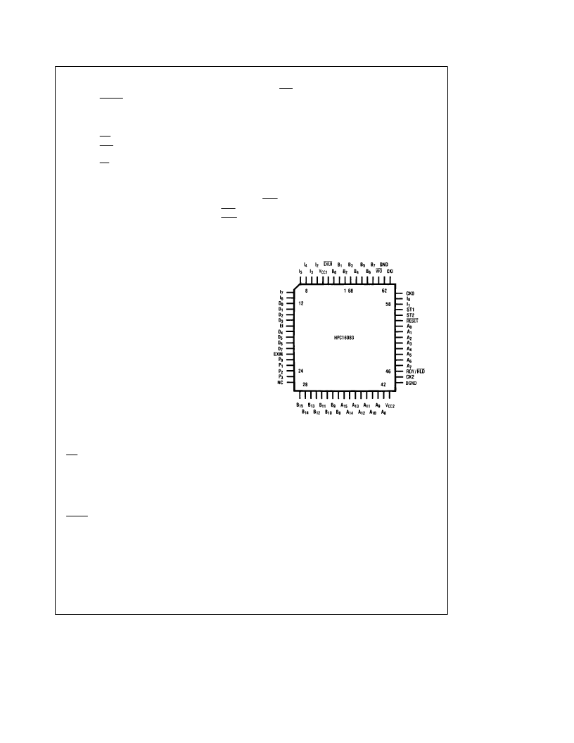
Connection Diagrams
Plastic and Ceramic Leaded Chip Carriers
TL/DD/8801–11
Top View
See NS Package Number EL68A or V68A
See Part Selection for Ordering Information
12
相關PDF資料 |
PDF描述 |
|---|---|
| HPC16004 | High-Performance microController |
| HPC16064 | High-Performance microController |
| HPC26004 | High-Performance microController |
| HPC26064 | High-Performance microController |
| HPC36004 | High-Performance microController |
相關代理商/技術參數 |
參數描述 |
|---|---|
| HPC26003E17 | 制造商:未知廠家 制造商全稱:未知廠家 功能描述:16-Bit Microcontroller |
| HPC26003E20 | 制造商:未知廠家 制造商全稱:未知廠家 功能描述:16-Bit Microcontroller |
| HPC26003E30 | 制造商:未知廠家 制造商全稱:未知廠家 功能描述:16-Bit Microcontroller |
| HPC26003EL20 | 制造商:未知廠家 制造商全稱:未知廠家 功能描述:16-Bit Microcontroller |
| HPC26003EL30 | 制造商:未知廠家 制造商全稱:未知廠家 功能描述:16-Bit Microcontroller |
發(fā)布緊急采購,3分鐘左右您將得到回復。