- 您現(xiàn)在的位置:買賣IC網(wǎng) > PDF目錄371881 > HPC26003 (National Semiconductor Corporation) High-Performance microControllers PDF資料下載
參數(shù)資料
| 型號: | HPC26003 |
| 廠商: | National Semiconductor Corporation |
| 英文描述: | High-Performance microControllers |
| 中文描述: | 高性能微控制器 |
| 文件頁數(shù): | 3/36頁 |
| 文件大小: | 467K |
| 代理商: | HPC26003 |
第1頁第2頁當前第3頁第4頁第5頁第6頁第7頁第8頁第9頁第10頁第11頁第12頁第13頁第14頁第15頁第16頁第17頁第18頁第19頁第20頁第21頁第22頁第23頁第24頁第25頁第26頁第27頁第28頁第29頁第30頁第31頁第32頁第33頁第34頁第35頁第36頁
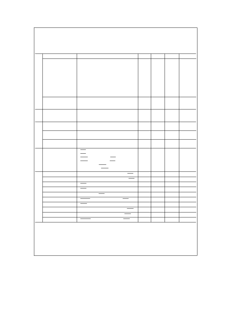
20 MHz
AC Electrical Characteristics
(See Notes 1 and 4 and Figure 1 thru Figure 5) V
CC
e
5.0V
g
10% unless otherwise specified, T
A
e
0
§
C to
a
70
§
C for
HPC46083/HPC46003,
b
40
§
C to
a
85
§
C for HPC36083/HPC36003,
b
40
§
C to
a
105
§
C for HPC26083/HPC26003,
b
55
§
C to
a
125
§
C for HPC16083/HPC16003
Symbol and Formula
Parameter
Min
Max
Units
Note
f
C
t
C1
e
1/f
C
t
CKIH
t
CKIL
t
C
e
2/f
C
t
WAIT
e
t
C
t
DC1C2R
CKI Operating Frequency
CKI Clock Period
CKI High Time
CKI Low Time
CPU Timing Cycle
CPU Wait State Period
Delay of CK2 Rising Edge after
CKI Falling Edge
Delay of CK2 Falling Edge after
CKI Falling Edge
2
20
500
MHz
ns
ns
ns
ns
ns
50
22.5
22.5
100
100
0
55
ns
(Note 2)
t
DC1C2F
0
55
ns
(Note 2)
f
U
e
f
C
/8
f
MW
External UART Clock Input Frequency
External MICROWIRE/PLUS
Clock Input Frequency
2.5
**
MHz
1.25
MHz
f
XIN
e
f
C
/22
t
XIN
e
t
C
External Timer Input Frequency
0.91
MHz
Pulse Width for Timer Inputs
100
ns
t
UWS
MICROWIRE Setup TimeDMaster
100
20
ns
DSlave
t
UWH
MICROWIRE Hold TimeDMaster
20
50
ns
DSlave
t
UWV
MICROWIRE Output Valid TimeDMaster
50
150
ns
DSlave
t
SALE
e
*/4
t
C
a
40
t
HWP
e
t
C
a
10
t
HAE
e
t
C
a
100
t
HAD
e
*/4
t
C
a
85
t
BF
e
(/2
t
C
a
66
t
BE
e
(/2
t
C
a
66
HLD Falling Edge before ALE Rising Edge
HLD Pulse Width
HLDA Falling Edge after HLD Falling Edge
HLDA Rising Edge after HLD Rising Edge
Bus Float after HLDA Falling Edge
Bus Enable after HLDA Rising Edge
115
110
ns
ns
ns
ns
ns
ns
200
160
116
(Note 3)
(Note 5)
(Note 5)
116
t
UAS
Address Setup Time to Falling Edge of URD
10
ns
t
UAH
Address Hold Time from Rising Edge of URD
10
ns
t
RPW
URD Pulse Width
100
ns
t
OE
URD Falling Edge to Output Data Valid
0
60
ns
t
OD
Rising Edge of URD to Output Data Invalid
5
35
ns
(Note 6)
t
DRDY
RDRDY Delay from Rising Edge of URD
70
ns
t
WDW
UWR Pulse Width
40
ns
t
UDS
Input Data Valid before Rising Edge of UWR
10
ns
t
UDH
Input Data Hold after Rising Edge of UWR
20
ns
t
A
WRRDY Delay from Rising Edge of UWR
70
ns
C
T
M
P
E
U
**
This maximum frequency is attainable provided that this external baud clock has a duty cycle such that the high period includes two (2) falling edges of the CK2
clock.
3
相關(guān)PDF資料 |
PDF描述 |
|---|---|
| HPC16004 | High-Performance microController |
| HPC16064 | High-Performance microController |
| HPC26004 | High-Performance microController |
| HPC26064 | High-Performance microController |
| HPC36004 | High-Performance microController |
相關(guān)代理商/技術(shù)參數(shù) |
參數(shù)描述 |
|---|---|
| HPC26003E17 | 制造商:未知廠家 制造商全稱:未知廠家 功能描述:16-Bit Microcontroller |
| HPC26003E20 | 制造商:未知廠家 制造商全稱:未知廠家 功能描述:16-Bit Microcontroller |
| HPC26003E30 | 制造商:未知廠家 制造商全稱:未知廠家 功能描述:16-Bit Microcontroller |
| HPC26003EL20 | 制造商:未知廠家 制造商全稱:未知廠家 功能描述:16-Bit Microcontroller |
| HPC26003EL30 | 制造商:未知廠家 制造商全稱:未知廠家 功能描述:16-Bit Microcontroller |
發(fā)布緊急采購,3分鐘左右您將得到回復(fù)。