- 您現(xiàn)在的位置:買賣IC網(wǎng) > PDF目錄370684 > HS3140B-883 14-Bit Multiplying DACs PDF資料下載
參數(shù)資料
| 型號(hào): | HS3140B-883 |
| 英文描述: | 14-Bit Multiplying DACs |
| 中文描述: | 14位乘法數(shù)模轉(zhuǎn)換器 |
| 文件頁(yè)數(shù): | 5/8頁(yè) |
| 文件大?。?/td> | 108K |
| 代理商: | HS3140B-883 |

Corporation
SIGNAL PROCESSING EXCELLENCE
163
2
-
1
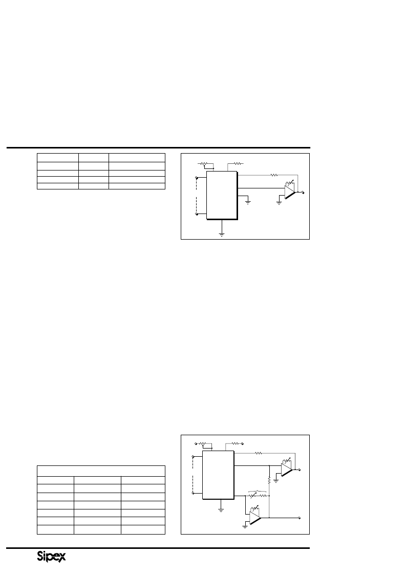
(MSB)
0
0
1
1
2
-
2
0
1
0
1
Output
0
1/4 Full-Scale
1/2 Full-Scale
3/4 Full-Scale
Table 1. Contribution of the two MSB's
VREF
VDD
470
DIGITAL
RFEEDBACK
IO1
+
-
IO2
GND
ROS
A
VOUT
SP7514
200
400
Figure 2. Unipolar Operation
accuracy required of any switch for a given overall
converter accuracy.
With the decoded converter described above, a 1%
change in any of the converter’s switches will affect
the output by no more than 0.25% of full-scale as
compared to 0.5% for a conventional converter. In
other words the conventional D/A converter can be
made less sensitive to the quality of its individual bits
by decoding.
In the
SP7514/HS3140
the first four MSB’s are
decoded into 16 levels which drive 15 equally weighted
current sources. The sensitivity of each switch on the
output is reduced by a factor of 8. Each of the 15
sources contributes 6.25% output change rather than
an MSB change of 50% for the common approach.
Following the decoded section of the DAC a standard
binary weighted R-2R approach is used. This divides
each of the 16 levels (or 6.25% of F.S.) into 4096
discrete levels (the 12 LSB’s).
Output Capacitance
The
SP7514/HS3140
have very low output capaci-
tance (C
). This is specified both with all switches ON
and all switches OFF. Output capacitance varies from
50pF to 100pF over all input codes. This low capaci-
tance is due in part to the decoding technique used.
Smaller switches are used with resulting less capaci-
tance. Three important system characteristics are
affected by C
O
and
C
O
; namely digital feedthrough,
settling time, and bandwidth. The DAC output equiva-
lent circuit can be represented as shown in
Figure 1
.
Digital feedthrough is the change in analog output due
to the toggling conditions on the converter input data
lines when the analog input V
is at 0V. The
SP7514/HS3140
very low C
and therefore will yield
low digital feedthrough. Inputs to the DAC can be
buffered. This input latch with microprocessor control
is shown in
Figure 4
.
Settling time is directly affected by C
. In
Figure 1
, C
O
combines with R
to add a pole to the open loop
response, reducing bandwidth and causing excessive
phase shift - which could result in ringing and/or
oscillation. A feedback capacitor, C
must be added to
restore stability. Even with C
, there is still a zero-pole
mismatch due to R
C
which is code dependent. This
code dependent mismatch is minimized when C
R
=
R
C
. However C
must now be made larger to
compensate for worst case
R
C
- resulting in re-
duced bandwidth and increased settling time. With the
SP7514/HS3140,
small values for C
f
must be used.
DIGITAL
RFEEDBACK
IO1
+
-
IO2
GND
ROS1
A
VOUT
1
+
-
A2
ROS2
VOUT1
A1, A2, OP-07
4K
4K
ROS2
R
200
VREF
VDD
470
400
SP7514
Figure 3. Bipolar Operation
TRANSFER FUNCTION (N=14)
BINARY INPUT UNIPOLAR OUTPUT BIPOLAR OUTPUT
111...111
–V
REF
(1 - 2
–N
)
–V
REF
(1/2 + 2
–N
)
–V
REF
/2
–V
REF
(1/2 – 2
–N
)
–V
REF
(2
(N – 1)
)
0
–V
REF
(1 – 2
–(N – 1)
)
–V
REF
(2
–(N – 1)
)
0
V
REF
(2
–(N – 1)
)
V
REF
(1 – 2
–(N – 1)
)
V
REF
100...001
100...000
011...111
000…001
000...000
Table 2. Transfer Function
相關(guān)PDF資料 |
PDF描述 |
|---|---|
| HS7514 | 14-Bit Multiplying DACs |
| HS3160B-3 | 16-Bit Digital-to-Analog Converter |
| HS3160B-4 | 16-Bit Digital-to-Analog Converter |
| HS3160C-3 | 16-Bit Digital-to-Analog Converter |
| HS3160C-4 | 16-Bit Digital-to-Analog Converter |
相關(guān)代理商/技術(shù)參數(shù) |
參數(shù)描述 |
|---|---|
| HS3140C-3 | 制造商:未知廠家 制造商全稱:未知廠家 功能描述:14-Bit Digital-to-Analog Converter |
| HS3140C-3Q | 制造商:SIPEX 制造商全稱:Sipex Corporation 功能描述:14-Bit Multiplying DACs |
| HS3140C-4 | 制造商:未知廠家 制造商全稱:未知廠家 功能描述:14-Bit Digital-to-Analog Converter |
| HS3140C-4Q | 制造商:SIPEX 制造商全稱:Sipex Corporation 功能描述:14-Bit Multiplying DACs |
| HS3-1420 | 制造商:OHIO BUCKEYE 功能描述: |
發(fā)布緊急采購(gòu),3分鐘左右您將得到回復(fù)。