- 您現(xiàn)在的位置:買賣IC網(wǎng) > PDF目錄371896 > HSP43216JC-52 (INTERSIL CORP) Halfband Filter PDF資料下載
參數(shù)資料
| 型號: | HSP43216JC-52 |
| 廠商: | INTERSIL CORP |
| 元件分類: | 數(shù)字信號處理外設(shè) |
| 英文描述: | Halfband Filter |
| 中文描述: | 16-BIT, DSP-DIGITAL FILTER, PQCC84 |
| 封裝: | PLASTIC, MS-018AF, LCC-84 |
| 文件頁數(shù): | 17/19頁 |
| 文件大小: | 144K |
| 代理商: | HSP43216JC-52 |
3-209
Absolute Maximum Ratings
Thermal Information
Supply Voltage. . . . . . . . . . . . . . . . . . . . . . . . . . . . . . . . . . . . . +7.0V
Input, Output or I/O Voltage. . . . . . . . . . . .GND -0.5V to V
CC
+0.5V
ESD Classification . . . . . . . . . . . . . . . . . . . . . . . . . . . . . . . . .Class 1
Operating Conditions
Voltage Range . . . . . . . . . . . . . . . . . . . . . . . . . . . .+4.75V to +5.25V
Temperature Range. . . . . . . . . . . . . . . . . . . . . . . . . . . .0
o
C to 70
o
C
Thermal Resistance (Typical, Note 1)
CPGA Package . . . . . . . . . . . . . . . . . .
PLCC Package. . . . . . . . . . . . . . . . . . .
MQFP Package . . . . . . . . . . . . . . . . . .
Maximum Junction Temperature
PLCC and MQFP Packages. . . . . . . . . . . . . . . . . . . . . . . . .150
o
C
CPGA Package . . . . . . . . . . . . . . . . . . . . . . . . . . . . . . . . . .175
o
C
Maximum Storage Temperature Range. . . . . . . . . . -65
o
C to 150
o
C
Maximum Lead Temperature (Soldering 10s) . . . . . . . . . . . . .300
o
C
(PLCC and MQFP Lead Tips Only)
θ
JA
(
o
C/W)
40
23.0
35.0
θ
JC
(
o
C/W)
8
N/A
N/A
Die Characteristics
Gate Count . . . . . . . . . . . . . . . . . . . . . . . . . . . . . . . . . .35469 Gates
CAUTION: Stresses above those listed in “Absolute Maximum Ratings” may cause permanent damage to the device. This is a stress only rating and operation of the
device at these or any other conditions above those indicated in the operational sections of this specification is not implied.
NOTE:
1.
θ
JA
is measured with the component mounted on an evaluation PC board in free air.
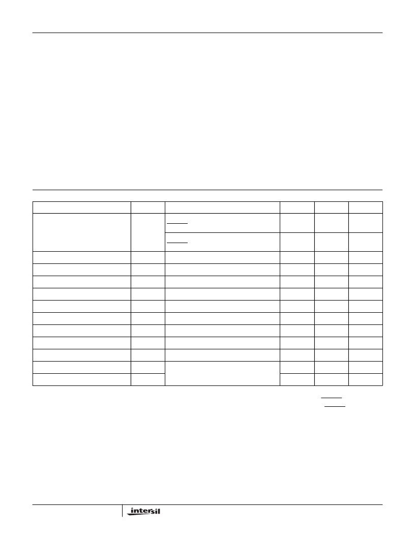
DC Electrical Specifications
V
CC
= 5.0V
±
5%, T
A
= 0
o
to 70
o
C
PARAMETER
SYMBOL
TEST CONDITIONS
MIN
MAX
UNITS
Power Supply Current
I
CCOP
V
CC
= Max, CLK Frequency 52MHz
INT/EXT = ‘1’, Notes 2, 4
-
468
mA
V
CC
= Max, CLK Frequency 52MHz
INT/EXT = ‘0’, Notes 3, 4
-
572
mA
Standby Power Supply Current
I
CCSB
V
CC
= Max, Outputs Not Loaded
-
500
μ
A
Input Leakage Current
I
I
V
CC
= Max, Input = 0V or V
CC
-10
10
μ
A
Output Leakage Current
I
O
V
CC
= Max, Input = 0V or V
CC
-10
10
μ
A
Clock Input High
V
IHC
V
CC
= Max
3.0
-
V
Clock Input Low
V
ILC
V
CC
= Min
-
0.8
V
Logical One Input Voltage
V
IH
V
CC
= Max
2.0
-
V
Logical Zero Input Voltage
V
IL
V
CC
= Min
-
0.8
V
Logical One Output Voltage
V
OH
I
OH
= -3mA, V
CC
= Min
2.6
-
V
Logical Zero Output Voltage
V
OL
I
OL
= 5mA, V
CC
= Min
-
0.4
V
Input Capacitance
C
IN
CLK Frequency 1MHz, All measurements ref-
erenced to GND. T
A
= 25
o
C, Note 5
-
12
pF
Output Capacitance
C
OUT
-
12
pF
NOTES:
2. Power supply current is proportional to frequency. Typical rating is 9mA/MHz when Internal Multiplexing is selected, INT/EXT = 1.
3. Power supply current is proportional to frequency. Typical rating is 11mA/MHz when External Multiplexing is selected, INT/EXT = 0.
4. Output load per test circuit and C
L
= 40pF.
5. Not tested, but characterized at initial design and at major process/design changes.
6. Maximum junction temperature must be considered when operating part at high clock frequencies.
HSP43216
相關(guān)PDF資料 |
PDF描述 |
|---|---|
| HSP43220JC-15 | Circular Connector; MIL SPEC:MIL-C-5015; Body Material:Metal; Series:GT; No. of Contacts:4; Connector Shell Size:24; Connecting Termination:Solder; Circular Shell Style:Box Mount Receptacle; Body Style:Straight |
| HSP43220GC-25 | Decimating Digital Filter |
| HSP43220GC-33 | Decimating Digital Filter |
| HSP43220VC-33 | Decimating Digital Filter |
| HSP43220 | RESISTOR 47 OHM 20W TO220 |
相關(guān)代理商/技術(shù)參數(shù) |
參數(shù)描述 |
|---|---|
| HSP43216JC-52S2485 | 制造商:Rochester Electronics LLC 功能描述:- Bulk |
| HSP43216JC-52Z | 功能描述:有源濾波器 W/ANNEAL HALFB& INTE RP/DECIMATE FILTER RoHS:否 制造商:Maxim Integrated 通道數(shù)量:1 截止頻率:150 KHz 電源電壓-最大:11 V 電源電壓-最小:4.74 V 最大工作溫度:+ 85 C 安裝風(fēng)格:Through Hole 封裝 / 箱體:PDIP N 封裝:Tube |
| HSP43216JI-52 | 制造商:Rochester Electronics LLC 功能描述:- Bulk |
| HSP43216VC-52 | 功能描述:有源濾波器 HALFBAND FILTER 100 PIN PQFP,COMM RoHS:否 制造商:Maxim Integrated 通道數(shù)量:1 截止頻率:150 KHz 電源電壓-最大:11 V 電源電壓-最小:4.74 V 最大工作溫度:+ 85 C 安裝風(fēng)格:Through Hole 封裝 / 箱體:PDIP N 封裝:Tube |
| HSP43216VC-52Z | 功能描述:有源濾波器 W/ANNEAL HALFB & FILER 100 PIN PQFP RoHS:否 制造商:Maxim Integrated 通道數(shù)量:1 截止頻率:150 KHz 電源電壓-最大:11 V 電源電壓-最小:4.74 V 最大工作溫度:+ 85 C 安裝風(fēng)格:Through Hole 封裝 / 箱體:PDIP N 封裝:Tube |
發(fā)布緊急采購,3分鐘左右您將得到回復(fù)。