- 您現(xiàn)在的位置:買賣IC網(wǎng) > PDF目錄371905 > HUF76121D3 (FAIRCHILD SEMICONDUCTOR CORP) 20A, 30V, 0.023 Ohm, N-Channel, Logic Level UltraFET Power MOSFETs PDF資料下載
參數(shù)資料
| 型號: | HUF76121D3 |
| 廠商: | FAIRCHILD SEMICONDUCTOR CORP |
| 元件分類: | 功率晶體管 |
| 英文描述: | 20A, 30V, 0.023 Ohm, N-Channel, Logic Level UltraFET Power MOSFETs |
| 中文描述: | 20 A, 30 V, 0.033 ohm, N-CHANNEL, Si, POWER, MOSFET, TO-251AA |
| 封裝: | TO-251AA, 3 PIN |
| 文件頁數(shù): | 8/11頁 |
| 文件大小: | 124K |
| 代理商: | HUF76121D3 |
8
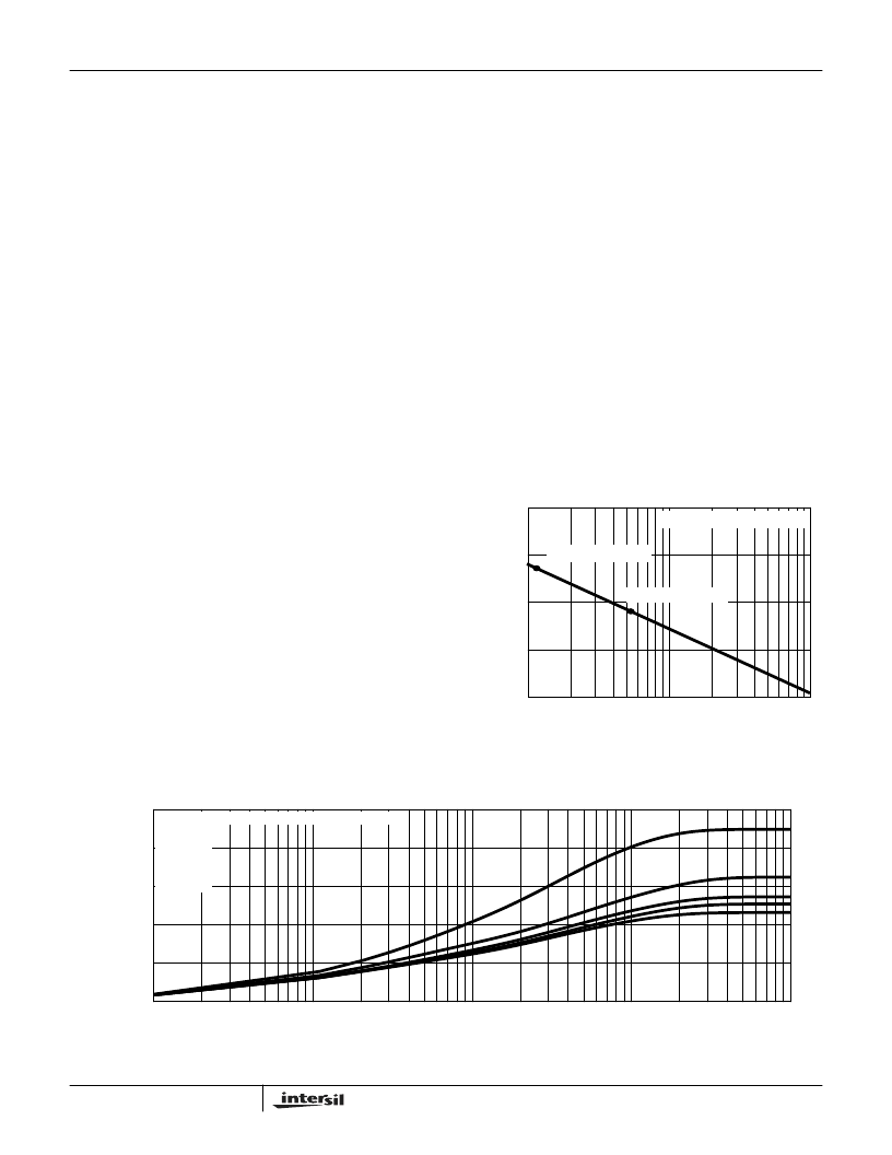
Thermal Resistance vs. Mounting Pad Area
The maximum rated junction temperature, T
JM
, and the ther-
mal resistance of the heat dissipating path determines the
maximum allowable device power dissipation, P
DM
, in an
application. Therefore the application’s ambient tempera-
ture, T
A
(
o
C), and thermal resistance R
θ
JA
(
o
C/W) must be
reviewed to ensure that T
JM
is never exceeded. Equation 1
mathematically represents the relationship and serves as
the basis for establishing the rating of the part.
In using surface mount devices such as the SOP-8 package,
the environment in which it is applied will have a significant
influence on the part’s current and maximum power
dissipation ratings. Precise determination of P
DM
is complex
and influenced by many factors:
1. Mounting pad area onto which the device is attached and
whether there is copper on one side or both sides of the
board.
2. The number of copper layers and the thickness of the
board.
3. The use of external heat sinks.
4. The use of thermal vias.
5. Air flow and board orientation.
6. For non steady state applications, the pulse width, the
duty cycle and the transient thermal response of the part,
the board and the environment they are in.
Intersil provides thermal information to assist the designer’s
preliminary application evaluation. Figure 23 defines the
R
θ
JA
for the device as a function of the top copper (compo-
nent side) area. This is for a horizontally positioned FR-4
board with 1oz copper after 1000 seconds of steady state
power with no air flow. This graph provides the necessary
information for calculation of the steady state junction tem-
perature or power dissipation. Pulse applications can be
evaluated using the Intersil device Spice thermal model or
manually utilizing the normalized maximum transient thermal
impedance curve.
Thermal resistances corresponding to other copper areas can
be obtained from Figure 23 or by calculation using Equation 2.
R
θ
JA
is defined as the natural log of the area times a cofficient
added to a constant. The area, in square inches is the top
copper area including the gate and source pads.
ln
×
–
=
The transient thermal impedance (Z
θ
JA
) is also effected by
varied top copper board area. Figure 24 shows the effect of
copper pad area on single pulse transient thermal
impedance. Each trace represents a copper pad area in
square inches corresponding to the descending list in the
graph. Spice and SABER thermal models are provided for
each of the listed pad areas.
Copper pad area has no perceivable effect on transient ther-
mal impedance for pulse widths less than 100ms. For pulse
widths less than 100ms the transient thermal impedance is
determined by the die and package. Therefore, CTHERM1
through CTHERM5 and RTHERM1 through RTHERM5
remain constant for each of the thermal models. A listing of
the model component values is available in Table 1.
(EQ. 1)
PDM
θ
JA
–
(
------------------------------
)
=
(EQ. 2)
R
θ
JA
83.2
23.6
Area
(
)
120
160
200
240
0.1
1.0
80
0.01
R
θ
JA
= 83.2 - 23.6*
ln
(AREA)
152
o
C/W - 0.054in
2
189
o
C/W - 0.0115in
2
R
θ
J
(
o
C
AREA, TOP COPPER AREA (in
2
)
FIGURE 23. THERMAL RESISTANCE vs MOUNTING PAD AREA
30
60
90
120
150
0
10
-1
10
0
10
1
10
2
10
3
FIGURE 24. THERMAL IMPEDANCE vs MOUNTING PAD AREA
t, RECTANGULAR PULSE DURATION (s)
Z
θ
J
,
COPPER BOARD AREA - DESCENDING ORDER
0.04 in
0.28 in
2
0.52 in
2
0.76 in
2
1.00 in
2
I
o
C
HUF76121SK8
相關PDF資料 |
PDF描述 |
|---|---|
| HUF76121D3S | 20A, 30V, 0.023 Ohm, N-Channel, Logic Level UltraFET Power MOSFETs |
| HUF76121P3 | 47A, 30V, 0.021 Ohm, N-Channel, Logic Level UltraFET Power MOSFETs |
| HUF76121S3S | 47A, 30V, 0.021 Ohm, N-Channel, Logic Level UltraFET Power MOSFETs |
| HUF76121S3ST | 47A, 30V, 0.021 Ohm, N-Channel, Logic Level UltraFET Power MOSFETs |
| HUF76129S3S | 56A, 30V, 0.016 Ohm, N-Channel, Logic Level UltraFET Power MOSFETs |
相關代理商/技術參數(shù) |
參數(shù)描述 |
|---|---|
| HUF76121D3S | 功能描述:MOSFET RoHS:否 制造商:STMicroelectronics 晶體管極性:N-Channel 汲極/源極擊穿電壓:650 V 閘/源擊穿電壓:25 V 漏極連續(xù)電流:130 A 電阻汲極/源極 RDS(導通):0.014 Ohms 配置:Single 最大工作溫度: 安裝風格:Through Hole 封裝 / 箱體:Max247 封裝:Tube |
| HUF76121D3ST | 功能描述:MOSFET USE 512-FDD6612A Logic Level N-Ch RoHS:否 制造商:STMicroelectronics 晶體管極性:N-Channel 汲極/源極擊穿電壓:650 V 閘/源擊穿電壓:25 V 漏極連續(xù)電流:130 A 電阻汲極/源極 RDS(導通):0.014 Ohms 配置:Single 最大工作溫度: 安裝風格:Through Hole 封裝 / 箱體:Max247 封裝:Tube |
| HUF76121P3 | 功能描述:MOSFET 47a 30V N-Ch MOSFET RoHS:否 制造商:STMicroelectronics 晶體管極性:N-Channel 汲極/源極擊穿電壓:650 V 閘/源擊穿電壓:25 V 漏極連續(xù)電流:130 A 電阻汲極/源極 RDS(導通):0.014 Ohms 配置:Single 最大工作溫度: 安裝風格:Through Hole 封裝 / 箱體:Max247 封裝:Tube |
| HUF76121S3 | 制造商:Rochester Electronics LLC 功能描述:- Bulk |
| HUF76121S3S | 功能描述:MOSFET RoHS:否 制造商:STMicroelectronics 晶體管極性:N-Channel 汲極/源極擊穿電壓:650 V 閘/源擊穿電壓:25 V 漏極連續(xù)電流:130 A 電阻汲極/源極 RDS(導通):0.014 Ohms 配置:Single 最大工作溫度: 安裝風格:Through Hole 封裝 / 箱體:Max247 封裝:Tube |
發(fā)布緊急采購,3分鐘左右您將得到回復。